TAC 14 ICS Digital platform progress Henrik Carling

- Slides: 16
TAC 14 - ICS Digital platform progress Henrik Carling 2016 -10 -06
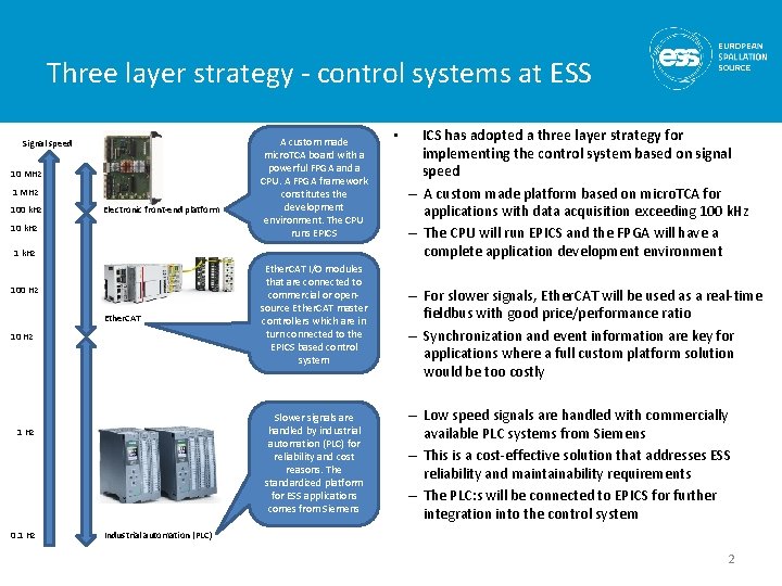
Three layer strategy - control systems at ESS Signal speed 10 MHz 100 k. Hz Electronic front-end platform 10 k. Hz A custom made micro. TCA board with a powerful FPGA and a CPU. A FPGA framework constitutes the development environment. The CPU runs EPICS 1 k. Hz 100 Hz Ether. CAT 10 Hz Slower signals are handled by industrial automation (PLC) for reliability and cost reasons. The standardized platform for ESS applications comes from Siemens 1 Hz 0. 1 Hz Ether. CAT I/O modules that are connected to commercial or opensource Ether. CAT master controllers which are in turn connected to the EPICS based control system • ICS has adopted a three layer strategy for implementing the control system based on signal speed – A custom made platform based on micro. TCA for applications with data acquisition exceeding 100 k. Hz – The CPU will run EPICS and the FPGA will have a complete application development environment – For slower signals, Ether. CAT will be used as a real-time fieldbus with good price/performance ratio – Synchronization and event information are key for applications where a full custom platform solution would be too costly – Low speed signals are handled with commercially available PLC systems from Siemens – This is a cost-effective solution that addresses ESS reliability and maintainability requirements – The PLC: s will be connected to EPICS for further integration into the control system Industrial automation (PLC) 2
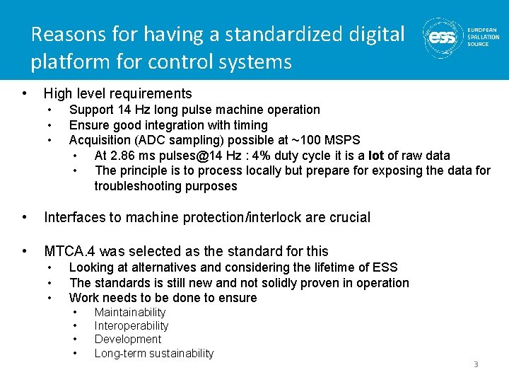
Reasons for having a standardized digital platform for control systems • High level requirements • • • Support 14 Hz long pulse machine operation Ensure good integration with timing Acquisition (ADC sampling) possible at ~100 MSPS • At 2. 86 ms pulses@14 Hz : 4% duty cycle it is a lot of raw data • The principle is to process locally but prepare for exposing the data for troubleshooting purposes • Interfaces to machine protection/interlock are crucial • MTCA. 4 was selected as the standard for this • • • Looking at alternatives and considering the lifetime of ESS The standards is still new and not solidly proven in operation Work needs to be done to ensure • • Maintainability Interoperability Development Long-term sustainability 3
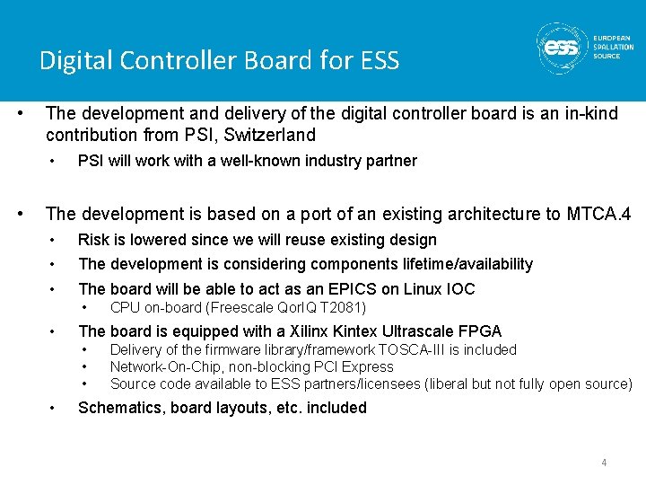
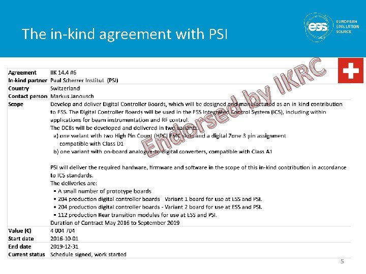
Digital Controller Board for ESS • The development and delivery of the digital controller board is an in-kind contribution from PSI, Switzerland • • PSI will work with a well-known industry partner The development is based on a port of an existing architecture to MTCA. 4 • • • Risk is lowered since we will reuse existing design The development is considering components lifetime/availability The board will be able to act as an EPICS on Linux IOC • • The board is equipped with a Xilinx Kintex Ultrascale FPGA • • CPU on-board (Freescale Qor. IQ T 2081) Delivery of the firmware library/framework TOSCA-III is included Network-On-Chip, non-blocking PCI Express Source code available to ESS partners/licensees (liberal but not fully open source) Schematics, board layouts, etc. included 4
The in-kind agreement with PSI C R K I y b d e s r o d En 5
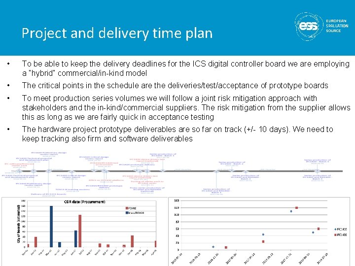
Project and delivery time plan • To be able to keep the delivery deadlines for the ICS digital controller board we are employing a ”hybrid” commercial/in-kind model • The critical points in the schedule are the deliveries/test/acceptance of prototype boards • To meet production series volumes we will follow a joint risk mitigation approach with stakeholders and the in-kind/commercial suppliers. The risk mitigation from the supplier allows this as long as we are fairly quick in acceptance testing • The hardware project prototype deliverables are so far on track (+/- 10 days). We need to keep tracking also firm and software deliverables 6
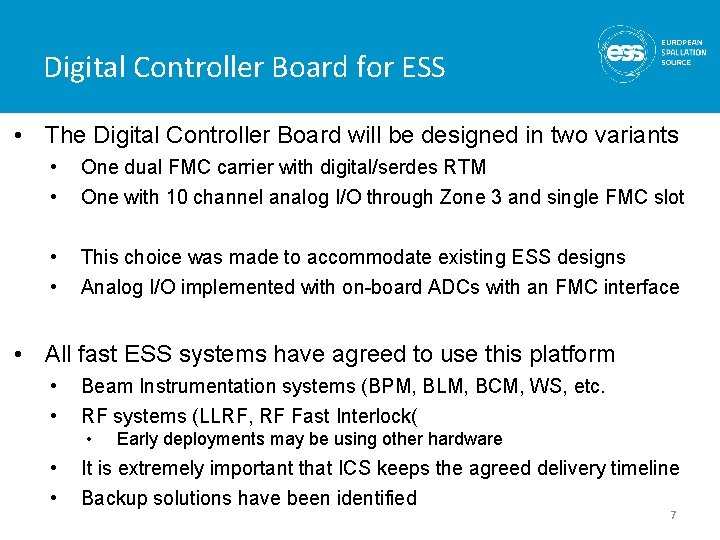
Digital Controller Board for ESS • The Digital Controller Board will be designed in two variants • • One dual FMC carrier with digital/serdes RTM One with 10 channel analog I/O through Zone 3 and single FMC slot • • This choice was made to accommodate existing ESS designs Analog I/O implemented with on-board ADCs with an FMC interface • All fast ESS systems have agreed to use this platform • • Beam Instrumentation systems (BPM, BLM, BCM, WS, etc. RF systems (LLRF, RF Fast Interlock( • • • Early deployments may be using other hardware It is extremely important that ICS keeps the agreed delivery timeline Backup solutions have been identified 7
IFC 1410 overview 8
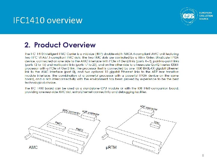
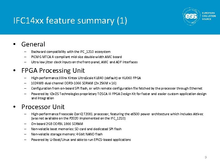
IFC 14 xx feature summary (1) • General – – – Backward compatibility with the IFC_1210 ecosystem PICMG MTCA. 4 -compliant mid-size double-width AMC board Ultra low jitter clock inputs on the front-panel, AMC and ADF interfaces • FPGA Processing Unit – – High-performance Xilinx Kintex Ultra. Scale KU 040 (default) or KU 060 FPGA 1024 MB dual channel DDR 3 -1066 SDRAM (2 x 256 M x 16) Configuration from on-board SPI flash, or with remote configuration file fetched by the processor through Ethernet Powered by IOx. OS Technologies proprietary TOSCA III FPGA Design Kit for faster and easier custom application design and integration • Processor Unit – – – High-performance Freescale Qor. IQ T 2081 processor, featuring the e 6500 power architecture which includes Altivec (was not available on the P 2020 implemented on the IFC_1210) On-board 2 GB DDR 3 L 1866 SDRAM Non-volatile boot memories: SD card and dedicated SPI flash Non-volatile storage memory: 4 Gbit NAND flash Powered by U-Boot/Linux and able to run EPICS-based applications 9
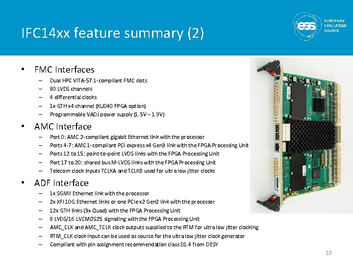
IFC 14 xx feature summary (2) • FMC Interfaces – – – Dual HPC VITA-57. 1 -compliant FMC slots 80 LVDS channels 4 differential clocks 1 x GTH x 4 channel (KU 040 FPGA option) Programmable VADJ power supply (1. 5 V – 1. 9 V) • AMC Interface – – – Port 0: AMC. 2 -compliant gigabit Ethernet link with the processor Ports 4 -7: AMC. 1 -compliant PCI express x 4 Gen 3 link with the FPGA Processing Unit Ports 12 to 15: point-to-point LVDS links with the FPGA Processing Unit Port 17 to 20: shared bus M-LVDS links with the FPGA Processing Unit Telecom clock inputs TCLKA and TCLKB used for ultra low jitter clocks • ADF Interface – – – – 1 x SGMII Ethernet link with the processor 2 x XFI 10 G Ethernet links or one PCIe x 2 Gen 2 link with the processor 12 x GTH links (3 x Quad) with the FPGA Processing Unit 8 LVDS/16 LVCMOS 25 signalling with the FPGA Processing Unit AMC_CLK and AMC_TCLK clock outputs supplied to the RTM for ultra low jitter clocking RTM_CLK clock input can be used as source for the ultra low jitter clock generator Compliant with pin assignment recommendation class D 1. 4 from DESY 10
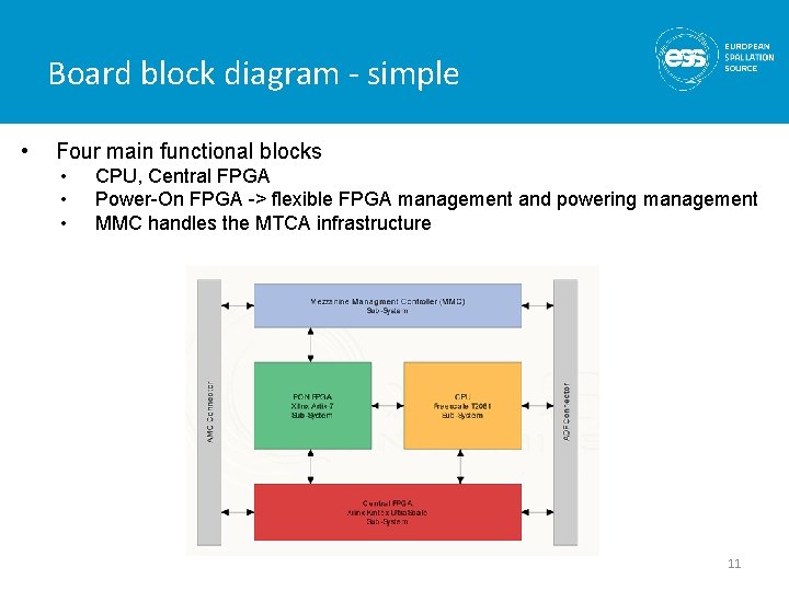
Board block diagram - simple • Four main functional blocks • • • CPU, Central FPGA Power-On FPGA -> flexible FPGA management and powering management MMC handles the MTCA infrastructure 11
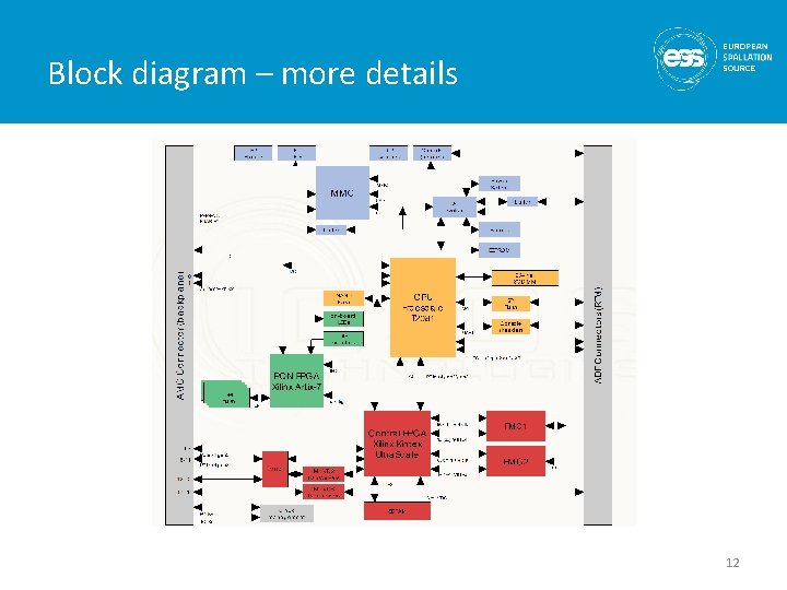
Block diagram – more details 12
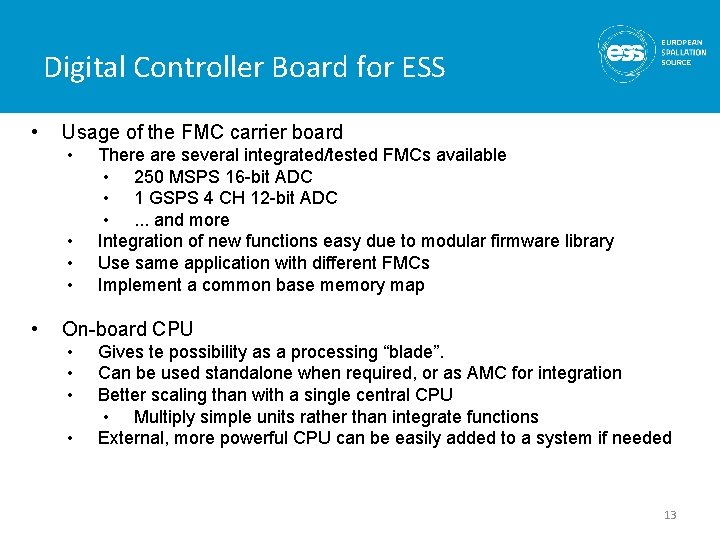
Digital Controller Board for ESS • Usage of the FMC carrier board • • • There are several integrated/tested FMCs available • 250 MSPS 16 -bit ADC • 1 GSPS 4 CH 12 -bit ADC • . . . and more Integration of new functions easy due to modular firmware library Use same application with different FMCs Implement a common base memory map On-board CPU • • Gives te possibility as a processing “blade”. Can be used standalone when required, or as AMC for integration Better scaling than with a single central CPU • Multiply simple units rather than integrate functions External, more powerful CPU can be easily added to a system if needed 13
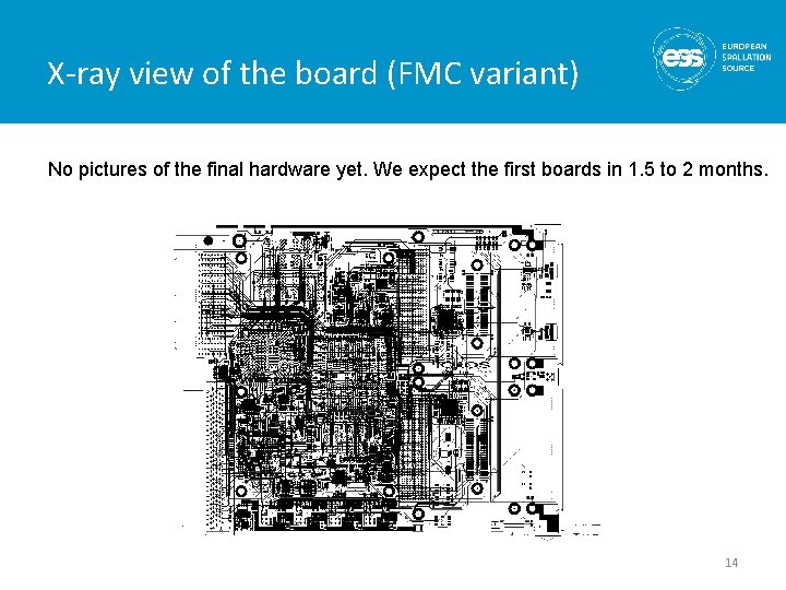
X-ray view of the board (FMC variant) No pictures of the final hardware yet. We expect the first boards in 1. 5 to 2 months. 14
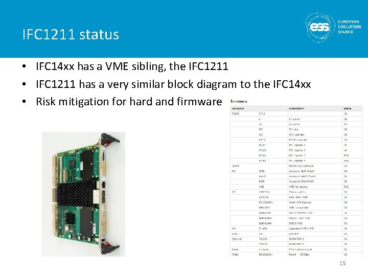
IFC 1211 status • IFC 14 xx has a VME sibling, the IFC 1211 • IFC 1211 has a very similar block diagram to the IFC 14 xx • Risk mitigation for hard and firmware 15
Thank you • Questions 16