Si PM from STMicroelectronics Nepomuk Otte Hector Romo
- Slides: 10

Si. PM from ST-Microelectronics Nepomuk Otte & Hector Romo Santa Cruz Institute for Particle Physics University of California, Santa Cruz nepomuk@scipp. ucsc. edu

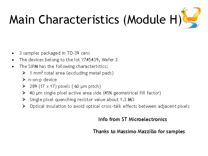
Main Characteristics (Module H) • • • 3 samples packaged in TO-39 cans The devices belong to the lot Y 745439, Wafer 3 The Si. PM has the following characteristics: Ø 1 mm 2 total area (excluding metal pads) Ø n-on-p device Ø 289 (17 x 17) pixels ( 60 µm pitch) Ø 40 µm single pixel active area side (45% geometrical fill factor) Ø Single pixel quenching resistor value about 1. 3 MΩ Ø Optical insulation to avoid optical cross-talk effects between adjacent pixels Info from ST Microelectronics Thanks to Massimo Mazzillo for samples

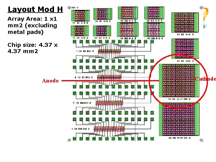
Layout Mod H Array Area: 1 x 1 mm 2 (excluding metal pads) Chip size: 4. 37 x 4. 37 mm 2 Anode Cathode

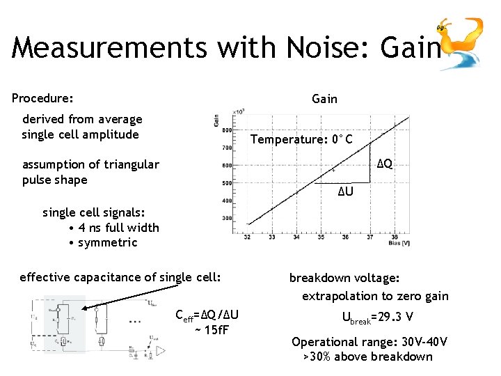
Measurements with Noise: Gain Procedure: Gain derived from average single cell amplitude Temperature: 0°C ΔQ assumption of triangular pulse shape ΔU single cell signals: • 4 ns full width • symmetric effective capacitance of single cell: Ceff=ΔQ/ΔU ~ 15 f. F breakdown voltage: extrapolation to zero gain Ubreak=29. 3 V Operational range: 30 V-40 V >30% above breakdown

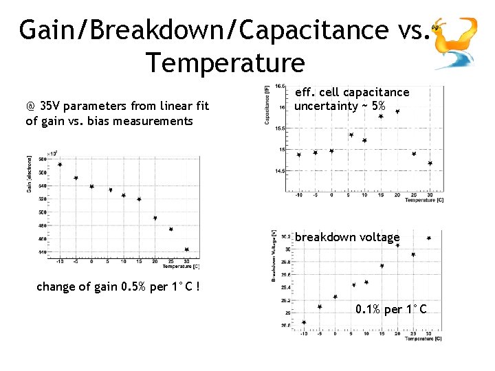
Gain/Breakdown/Capacitance vs. Temperature @ 35 V parameters from linear fit of gain vs. bias measurements eff. cell capacitance uncertainty ~ 5% breakdown voltage change of gain 0. 5% per 1°C ! 0. 1% per 1°C

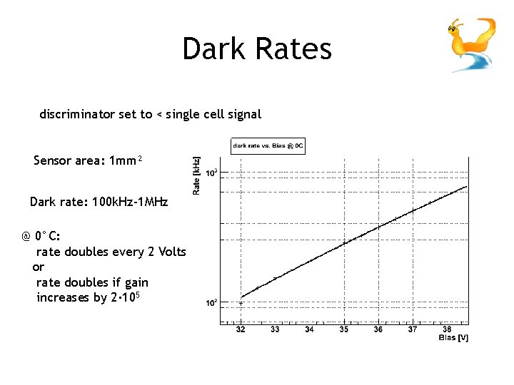
Dark Rates discriminator set to < single cell signal Sensor area: 1 mm² Dark rate: 100 k. Hz-1 MHz @ 0°C: rate doubles every 2 Volts or rate doubles if gain increases by 2· 105

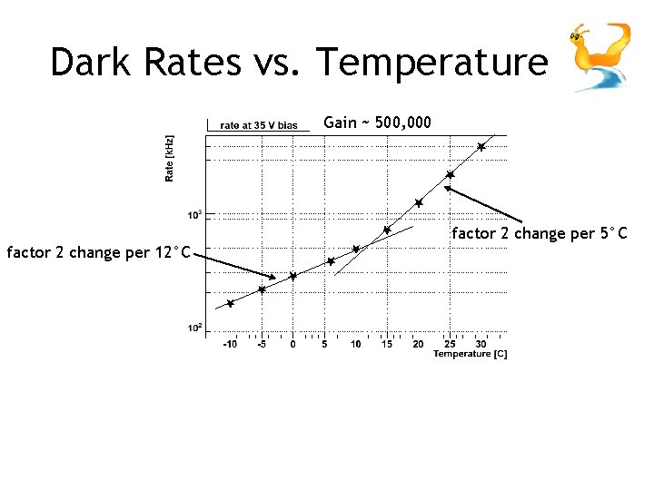
Dark Rates vs. Temperature Gain ~ 500, 000 factor 2 change per 12°C factor 2 change per 5°C

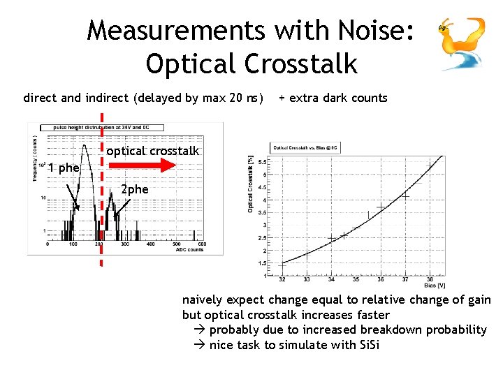
Measurements with Noise: Optical Crosstalk direct and indirect (delayed by max 20 ns) + extra dark counts optical crosstalk 1 phe 2 phe naively expect change equal to relative change of gain but optical crosstalk increases faster probably due to increased breakdown probability nice task to simulate with Si. Si

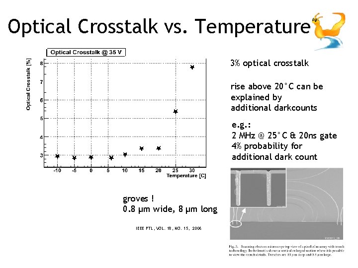
Optical Crosstalk vs. Temperature 3% optical crosstalk rise above 20°C can be explained by additional darkcounts e. g. : 2 MHz @ 25°C & 20 ns gate 4% probability for additional dark count groves ! 0. 8 µm wide, 8 µm long IEEE PTL, VOL. 18, NO. 15, 2006

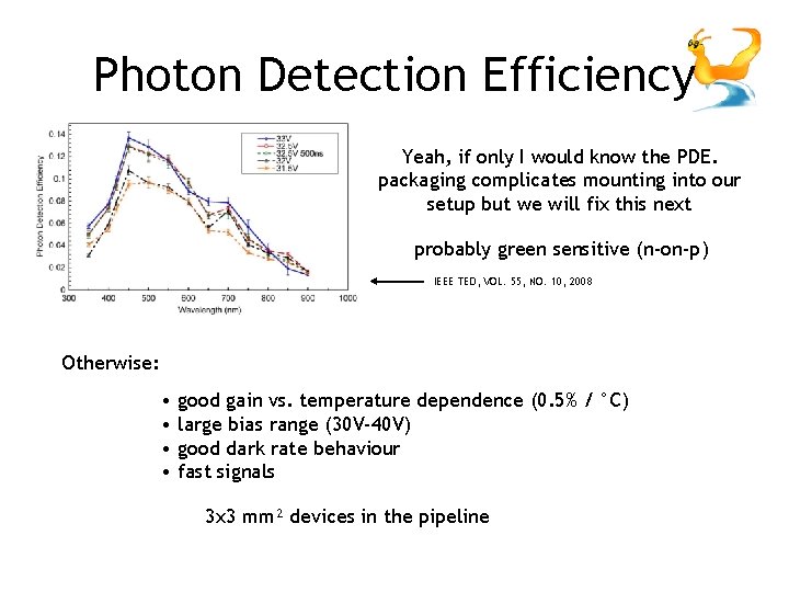
Photon Detection Efficiency Yeah, if only I would know the PDE. packaging complicates mounting into our setup but we will fix this next probably green sensitive (n-on-p) IEEE TED, VOL. 55, NO. 10, 2008 Otherwise: • good gain vs. temperature dependence (0. 5% / °C) • large bias range (30 V-40 V) • good dark rate behaviour • fast signals 3 x 3 mm² devices in the pipeline