Si and Ga N for large fluence irradiation
- Slides: 15

Si and Ga. N for large fluence irradiation monitoring J. Vaitkus 1, E. Gaubas 1, T. Ceponis 1, D. Meskauskaite 1, J. Pavlov 1, V. Rumbauskas 1, 2, F. Ravotti 2 M. Moll 1 Vilnius University, Institute of Photonics and Nanotechnology 2 CERN Outline: • • Motivation Samples and irradiations, anneals Measurement Techniques: Temperature dependent carrier trapping lifetime (TDTL), Pulsed photoionization spectroscopy (PPIS), Deep-level transient spectroscopy (DLTS) Results on Fz and Cz Si irradiated by electrons and hadrons Results on multicrystaline Si irradiated by 8 Me. V protons Results on Ga. N irradiated by 1 Me. V neutrons Commercial Ga. N LED structures as dosimeters of 1. 6 Me. V proton irradiation Summary

Our work is based on these effects: Comparison of characteristics of the pion, neutron and proton as irradiated and isothermally (Tan =80 C) annealed Si Comparison of exciton spectra in SI-Ga. N (MOCVD) irradiatet to different hadron fluence. Guenakh. Fest, University of Florida

J. Vaitkus│Si and Ga. N for large fluence irradiation monitoring│AIDA-2020 WP 15│2018 Motivation ● The better understanding of radiation damage of Si particle detectors is important in order: ● to extend sensor lifetime and their radiation hardness or ● to restore their functionality after degradation caused by irradiations − one of the ways to recover detector operational features is heat treatment at technically acceptable temperatures. ● Multicrystalline silicon (mc-Si) use for the detection of charged particles − inexpensive material for mass production. ● Semi-insulating Ga. N is a promising material for particle tracking detectors and for imaging detectors − there still remains a lack of detailed studies of the defects in the as-grown material and their interaction with radiation induced defects, particularly in heavily irradiated samples. 3

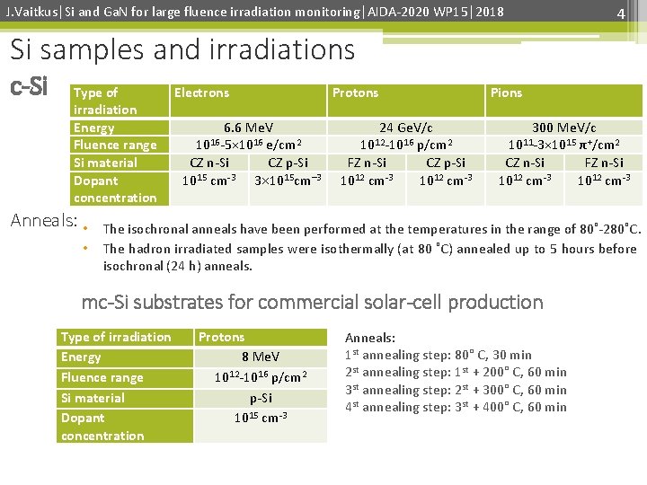
J. Vaitkus│Si and Ga. N for large fluence irradiation monitoring│AIDA-2020 WP 15│2018 4 Si samples and irradiations c-Si Type of irradiation Energy Fluence range Si material Dopant concentration Anneals: • • Electrons 6. 6 Me. V 1016 -5× 10¹⁶ e/cm 2 CZ n-Si CZ p-Si 1015 cm-3 3 1015 cm 3 Protons 24 Ge. V/c 1012 -1016 p/cm 2 FZ n-Si CZ p-Si 1012 cm-3 Pions 300 Me. V/c 1011 -3× 10¹⁵ π+/cm 2 CZ n-Si FZ n-Si 1012 cm-3 The isochronal anneals have been performed at the temperatures in the range of 80˚-280˚C. The hadron irradiated samples were isothermally (at 80 ˚C) annealed up to 5 hours before isochronal (24 h) anneals. mc-Si substrates for commercial solar-cell production Type of irradiation Energy Fluence range Si material Dopant concentration Protons 8 Me. V 1012 -1016 p/cm 2 p-Si 1015 cm-3 Anneals: 1 st annealing step: 80° C, 30 min 2 st annealing step: 1 st + 200° C, 60 min 3 st annealing step: 2 st + 300° C, 60 min 4 st annealing step: 3 st + 400° C, 60 min

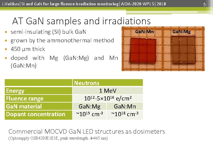
J. Vaitkus│Si and Ga. N for large fluence irradiation monitoring│AIDA-2020 WP 15│2018 5 AT Ga. N samples and irradiations • • semi-insulating (SI) bulk Ga. N grown by the ammonothermal method 450 µm thick doped with Mg (Ga. N: Mg) and Mn (Ga. N: Mn) Energy Fluence range Ga. N material Dopant concentration Ga. N: Mn Neutrons 1 Me. V 1012 -5× 10¹⁶ e/cm 2 Ga. N: Mg Ga. N: Mn ~1019 cm-3 ~1018 cm-3 Commercial MOCVD Ga. N LED structures as dosimeters (Optosupply OSB 4 XNE 1 E 1 E, peak wavelength =465 nm) Ga. N: Mg

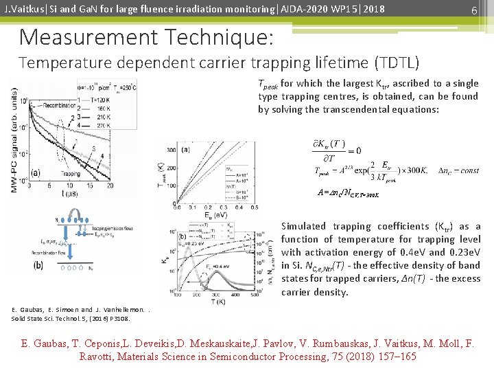
J. Vaitkus│Si and Ga. N for large fluence irradiation monitoring│AIDA-2020 WP 15│2018 6 Measurement Technique: Temperature dependent carrier trapping lifetime (TDTL) Tpeak for which the largest Ktr, ascribed to a single type trapping centres, is obtained, can be found by solving the transcendental equations: A= n. C/NC, V, T=300 K Simulated trapping coefficients (Ktr) as a function of temperature for trapping level with activation energy of 0. 4 e. V and 0. 23 e. V in Si. NC, e, Ntr(T) - the effective density of band states for trapped carriers, ∆n(T) - the excess carrier density. E. Gaubas, E. Simoen and J. Vanhellemon. . Solid State Sci. Technol. 5, (2016) P 3108. E. Gaubas, T. Ceponis, L. Deveikis, D. Meskauskaite, J. Pavlov, V. Rumbauskas, J. Vaitkus, M. Moll, F. Ravotti, Materials Science in Semiconductor Processing, 75 (2018) 157– 165

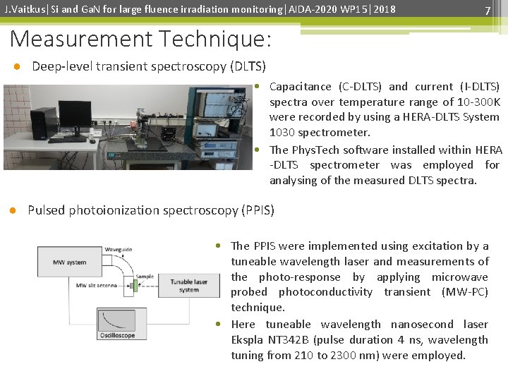
J. Vaitkus│Si and Ga. N for large fluence irradiation monitoring│AIDA-2020 WP 15│2018 7 Measurement Technique: ● Deep-level transient spectroscopy (DLTS) • Capacitance (C-DLTS) and current (I-DLTS) spectra over temperature range of 10 -300 K were recorded by using a HERA-DLTS System 1030 spectrometer. • The Phys. Tech software installed within HERA -DLTS spectrometer was employed for analysing of the measured DLTS spectra. ● Pulsed photoionization spectroscopy (PPIS) • The PPIS were implemented using excitation by a tuneable wavelength laser and measurements of the photo-response by applying microwave probed photoconductivity transient (MW-PC) technique. • Here tuneable wavelength nanosecond laser Ekspla NT 342 B (pulse duration 4 ns, wavelength tuning from 210 to 2300 nm) were employed.

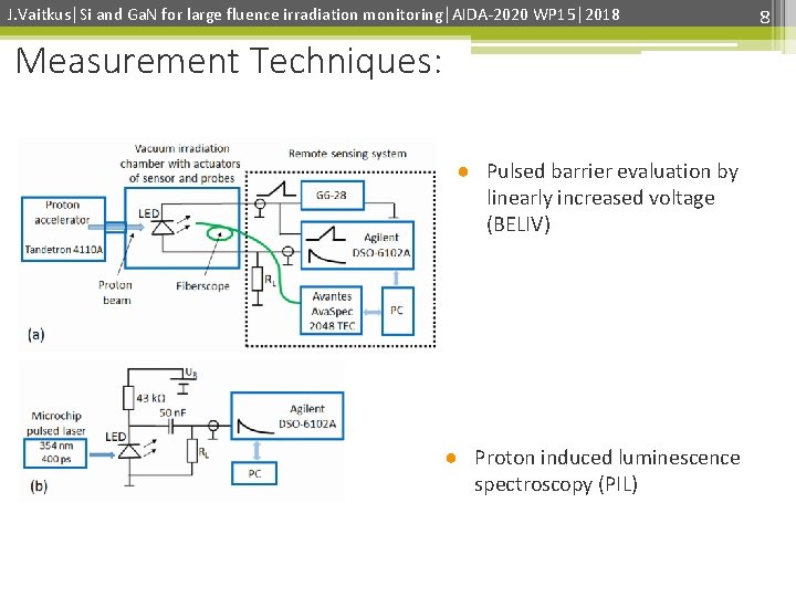
J. Vaitkus│Si and Ga. N for large fluence irradiation monitoring│AIDA-2020 WP 15│2018 Measurement Techniques: ● Pulsed barrier evaluation by linearly increased voltage (BELIV) ● Proton induced luminescence spectroscopy (PIL) 8

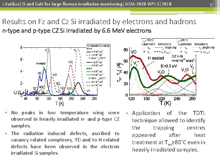
J. Vaitkus│Si and Ga. N for large fluence irradiation monitoring│AIDA-2020 WP 15│2018 Results on Fz and Cz Si irradiated by electrons and hadrons n-type and p-type CZ Si irradiated by 6. 6 Me. V electrons • No peaks in low temperature wing were observed in heavily irradiated n- and p-type CZ samples. • The radiation induced defects, ascribed to vacancy related complexes, TD and to H related defects have been observed in the electron irradiated Si samples. • Application of the TDTL technique allowed to identify the trapping centres appeared after heat treatment at Tan≥ 80˚C even in heavily irradiated samples. 9

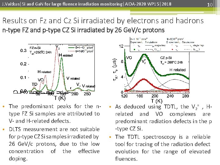
J. Vaitkus│Si and Ga. N for large fluence irradiation monitoring│AIDA-2020 WP 15│2018 10 Results on Fz and Cz Si irradiated by electrons and hadrons n-type FZ and p-type CZ Si irradiated by 26 Ge. V/c protons • The predominant peaks for the ntype FZ Si samples are attributed to V- and H-related defects. • DLTS measurement are not suitable for p-type CZ Si samples irradiated by 26 Ge. V/c protons, due to the low concentration of the effective doping. • As deduced using TDTL, the V 2= , Hrelated and VO complexes are predominant radiation defects in the p -type CZ Si. • The TDTL spectroscopy is a reliable tool for tracing of the radiation defect evolution for the range of elevated fluences.

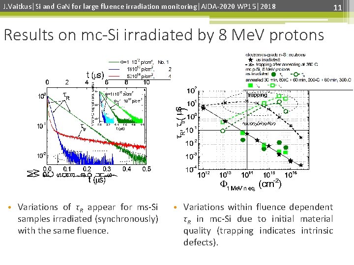
J. Vaitkus│Si and Ga. N for large fluence irradiation monitoring│AIDA-2020 WP 15│2018 Results on mc-Si irradiated by 8 Me. V protons • Variations of τR appear for ms-Si samples irradiated (synchronously) with the same fluence. • Variations within fluence dependent τR in mc-Si due to initial material quality (trapping indicates intrinsic defects). 11

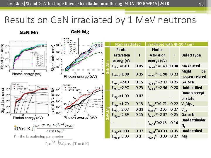
J. Vaitkus│Si and Ga. N for large fluence irradiation monitoring│AIDA-2020 WP 15│2018 12 Results on Ga. N irradiated by 1 Me. V neutrons Ga. N: Mg Ga. N: Mn • Non-irradiated Photoactivation Γ energy (e. V) EMn-1=1. 40 0. 05 EMn-2=1. 98 0. 25 EMn-3=2. 40 EMn-4=2. 97 0. 15 0. 25 EMg-1=1. 30 0. 02 EMg-2=1. 70 EMg-3=2. 07 EMg-4=2. 39 0. 15 0. 23 0. 15 − − EMg-5=3. 00 EMg-6=3. 30 0. 32 0. 2 Irradiated with Φ=1016 cm-2 Photoactivation Γ Defect type energy (e. V) EMn-1 irr=1. 42 0. 08 Mn related Might be EMn-2 irr=1. 98 0. 22 oxygen related EMn-3 irr=2. 37 0. 25 Ga. I or NI EMn-4 irr=2. 96 0. 28 Unidentified Donor/accept − − or state irr EMg-1 =1. 71 0. 22 VNMg. Ga EMg-2 irr=2. 05 0. 27 VGa EMn-3 irr=2. 37 0. 25 Ga. I or NI Unidentifiedor EMg-4 irr=2. 45 0. 16 NI irr EMg-5 =3. 00 0. 35 Unidentified EMg-6 irr=3. 30 0. 27 Mg. I

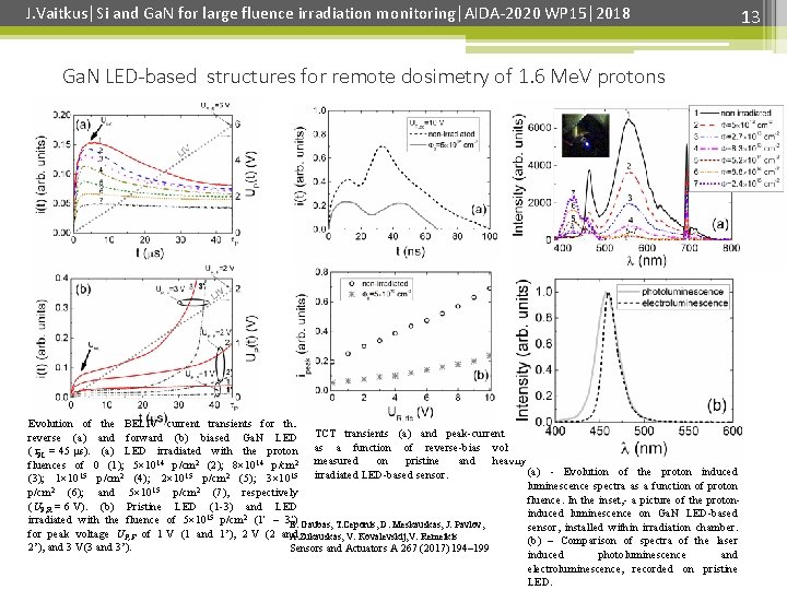
J. Vaitkus│Si and Ga. N for large fluence irradiation monitoring│AIDA-2020 WP 15│2018 Ga. N LED-based structures for remote dosimetry of 1. 6 Me. V protons Evolution of the BELIV current transients for the reverse (a) and forward (b) biased Ga. N LED TCT transients (a) and peak-current (b) ( PL = 45 s). (a) LED irradiated with the proton as a function of reverse-bias voltage on pristine and heavily fluences of 0 (1); 5 1014 p/cm 2 (2); 8 1014 p/cm 2 measured (a) - Evolution of the proton induced irradiated LED-based sensor. 15 2 15 (3); 1 10 p/cm (4); 2 10 p/cm (5); 3 10 luminescence spectra as a function of proton p/cm 2 (6); and 5 1015 p/cm 2 (7), respectively fluence. In the inset, - a picture of the proton(UP, R = 6 V). (b) Pristine LED (1 -3) and LED induced luminescence on Ga. N LED-based irradiated with the fluence of 5 1015 p/cm 2 (1 – 3 ) E. Gaubas, T. Ceponis, D. Meskauskas, J. Pavlov, sensor, installed within irradiation chamber. for peak voltage UP, F of 1 V (1 and 1’), 2 V (2 and A. Zukauskas, V. Kovalevskij, V. Remeikis (b) – Comparison of spectra of the laser 2’), and 3 V(3 and 3’). Sensors and Actuators A 267 (2017) 194– 199 induced photoluminescence and electroluminescence, recorded on pristine LED. 13

J. Vaitkus│Si and Ga. N for large fluence irradiation monitoring│AIDA-2020 WP 15│2018 Summary Ø The non-monotonous variations of trap densities after different anneal steps have been identified in heavily electrons and hadrons irradiated silicon by combining the DLTS and TDTL spectroscopy. Ø The similarity between DLTS spectra, obtained for rather low fluence irradiations by protons and pions, indicate that the irradiation with various type penetrative hadrons induce the same defects (the oxygen, vacancy and hydrogen related complexes and TD). Ø Contactless TDTL technique allows simultaneous control of interactions among several radiation defects within large fluences irradiated Si structures. Ø The AT-Ga. N material performance showed insignificant changes after neutron irradiation with large fluences (up to 5 1016 e/cm 2 ). Ø Ga. N LED-based sensors can be used for the synchronous detection of hadron irradiation by recording the optical (B-L) and electrical signals (ISC and TCT transients). 14

J. Vaitkus│Si and Ga. N for large fluence irradiation monitoring│AIDA-2020 WP 15│2018 Thank you for your attention! Acknowledgments ● This research was implemented according to AIDA-2020 TNA grants. This study was partially supported by Lithuanian Academy of Sciences, grants LMA-CERN-2017/2018. The work was partly performed in the framework of the CERN RD 50 collaboration. ● Authors are also indebted for pion irradiations performed at the proton accelerator, Paul Scherrer Institute, Villigen, Switzerland for electron irradiations performed at the Institute of Solid State and Semiconductor Physics, Minsk, Belarus.