Session1 Design with PLDs and FPGAs Course Name
- Slides: 9

Session-1 Design with PLDs and FPGAs Course Name “Design with PLDs & FPGAs” Course Code: 11 -EC-312 L-T-P: 3 -0 -2 Credits: 4 Dept of ECM

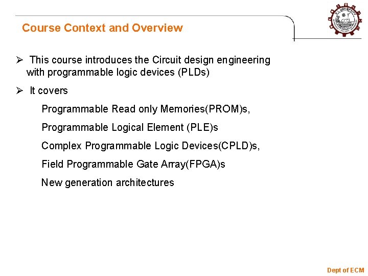
Course Context and Overview Ø This course introduces the Circuit design engineering with programmable logic devices (PLDs) Ø It covers Programmable Read only Memories(PROM)s, Programmable Logical Element (PLE)s Complex Programmable Logic Devices(CPLD)s, Field Programmable Gate Array(FPGA)s New generation architectures Dept of ECM

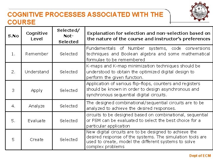
COGNITIVE PROCESSES ASSOCIATED WITH THE COURSE S. No 1. Cognitive Level Remember Selected/ Not. Selected Explanation for selection and non-selection based on the nature of the course and instructor’s preferences Selected Fundamentals of Number systems, code conversions techniques and Boolean algebra and some mathematical formulae to be remembered 2. Understand Selected 3 Apply Selected 4. Analyze Selected 5. Evaluate Selected 5 Create Selected K-maps and K-map minimization techniques should be understood to obtain the optimized digital design to perform the given function. Application of various flip-flops, counters and registers should be known in order to design asynchronous and synchronous sequential digital circuits. The designed combinational/sequential circuits are to be analyzed to achieve the desired responses. circuits to be designed based on combinational, sequential or FSM can be evaluated to select the best choice for a particular application New digital circuits are to be designed to achieve the desired response of the systems. The simulation tools are used to create, model the different systems to solve complex problems Dept of ECM

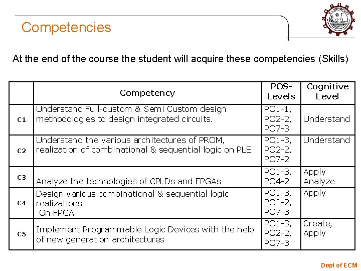
Competencies At the end of the course the student will acquire these competencies (Skills) Competency C 1 Understand Full-custom & Semi Custom design methodologies to design integrated circuits. C 2 Understand the various architectures of PROM, realization of combinational & sequential logic on PLE C 3 Analyze the technologies of CPLDs and FPGAs C 4 Design various combinational & sequential logic realizations On FPGA C 5 Implement Programmable Logic Devices with the help of new generation architectures POSLevels PO 1 -1, PO 2 -2, PO 7 -3 PO 1 -3, PO 2 -2, PO 7 -2 PO 1 -3, PO 4 -2 PO 1 -3, PO 2 -2, PO 7 -3 Cognitive Level Understand Apply Analyze Apply Create, Apply Dept of ECM

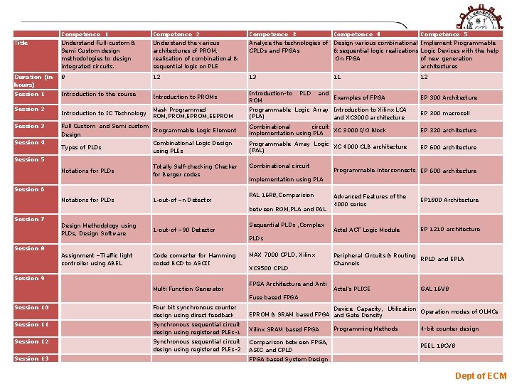
Competence 1 Understand Full-custom & Semi Custom design methodologies to design integrated circuits. Competence 2 Understand the various architectures of PROM, realization of combinational & sequential logic on PLE Competence 3 Analyze the technologies of CPLDs and FPGAs Competence 4 Design various combinational & sequential logic realizations On FPGA Competence 5 Implement Programmable Logic Devices with the help of new generation architectures Duration (in hours) 8 12 13 11 12 Session 1 Introduction to the course Introduction to PROMs Introduction-to ROM Examples of FPGA EP 300 Architecture Mask Programmed ROM, PROM, EEPROM Programmable Logic Array Introduction to Xilinx LCA (PLA) and XC 3000 architecture EP 300 macrocell Combinational circuit XC 3000 I/O Block implementation using PLA EP 320 architecture EP 600 architecture Title Session 2 Session 3 Session 4 Introduction to IC Technology Full Custom and Semi custom Programmable Logic Element Design PLD and Types of PLDs Combinational Logic Design using PLEs Programmable Array Logic XC 4000 CLB architecture (PAL) Notations for PLDs Totally Self-checking Checker for Berger codes Combinational circuit Session 5 Session 6 Notations for PLDs 1 -out-of –n Detector PAL 16 R 8, Comparision between ROM, PLA and PAL Session 7 Design Methodology using PLDs, Design Software 1 -out-of – 90 Detector Assignment –Traffic light controller using ABEL Code converter for Hamming coded BCD to ASCII Programmable interconnects EP 600 architecture implementation using PLA Sequential PLDs , Complex Advanced Features of the 4000 series EP 1800 Architecture Actel ACT Logic Module EP 1210 architecture PLDs Session 8 Session 9 Multi Function Generator MAX 7000 CPLD, Xilinx XC 9500 CPLD FPGA Architecture and Anti Peripheral Circuits & Routing RPLD and EPLA Channels Actel’s PLICE GAL 16 V 8 Fuse based FPGA Session 10 Four bit synchronous counter design using direct feedback Device Capacity, Utilization Operation modes of OLMCs EPROM & SRAM based FPGA and Gate Density Session 11 Synchronous sequential circuit design using registered PLEs-1 Xilinx SRAM based FPGA Session 12 Synchronous sequential circuit design using registered PLEs-2 Comparison between FPGA, ASIC and CPLD Session 13 Programming Methods 4 -bit counter design PEEL 18 CV 8 FPGA based System Design Dept of ECM

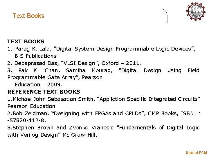
Text Books TEXT BOOKS 1. Parag K. Lala, “Digital System Design Programmable Logic Devices”, B S Publications 2. Debaprasad Das, “VLSI Design”, Oxford – 2011. 3. Pak K. Chan, Samiha Mourad, “Digital Design Using Field Programmable Gate Array”, Pearson Education – 2009. REFERENCE TEXT BOOKS 1. Michael John Sebasatian Smith, “Appliction Specific Integrated Circuits” Pearson Education 2. Bob Zeidman, “Designing with FPGAs and CPLDs”, CMP Books, ISBN: 1 -57820 -112 -8. 3. Stephen Brown and Zvonko Vranesic “Fundamentals of Digital Logic with Verilog Design” Mc Graw-Hill. Dept of ECM

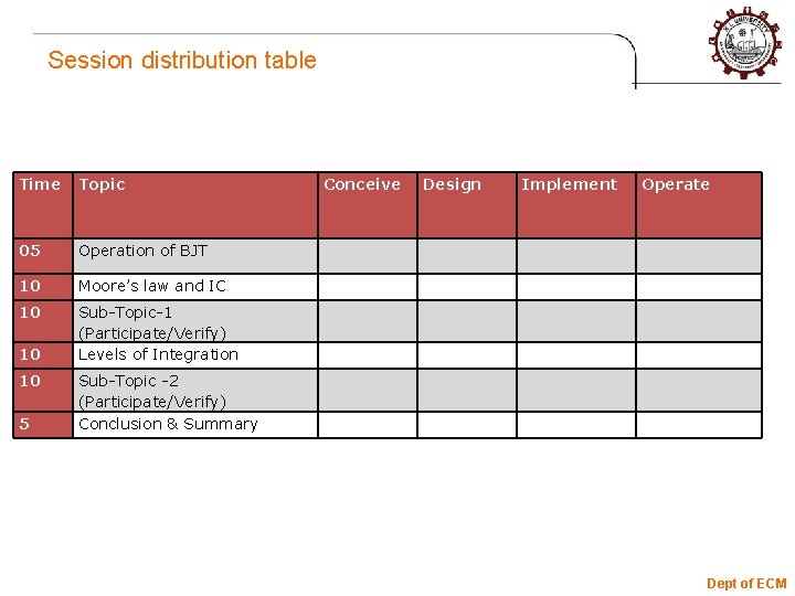
Session distribution table Time Topic 05 Operation of BJT 10 Moore’s law and IC 10 Sub-Topic-1 (Participate/Verify) Levels of Integration 10 10 5 Conceive Design Implement Operate Sub-Topic -2 (Participate/Verify) Conclusion & Summary Dept of ECM

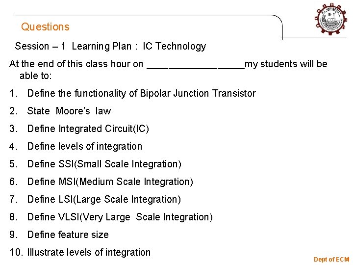
Questions Session – 1 Learning Plan : IC Technology At the end of this class hour on _________my students will be able to: 1. Define the functionality of Bipolar Junction Transistor 2. State Moore’s law 3. Define Integrated Circuit(IC) 4. Define levels of integration 5. Define SSI(Small Scale Integration) 6. Define MSI(Medium Scale Integration) 7. Define LSI(Large Scale Integration) 8. Define VLSI(Very Large Scale Integration) 9. Define feature size 10. Illustrate levels of integration Dept of ECM

Introduction to Digital circuits ØLogic gates Ø Basic gates Ø Universal gates ØCombinational circuits Ø Half adder Ø Full adder ØSequential circuits Ø Latches Ø Flip flops Dept of ECM