Piezo MEMS Foundry Naomi Montross Joe Evans Gerald
- Slides: 19

Piezo. MEMS Foundry Naomi Montross, Joe Evans, Gerald Salazar, Spencer Smith, Bob Howard, Radiant Technologies, Inc. 2019 International Workshop on Acoustic Transduction Materials and Devices May 7, 2018 Advanced Systems Test

Radiant Technologies has completed the first test wafer of its I-Beam piezo. MEMS process. Radiant will accept capacitor or piezo. MEMS foundry projects from universities and organizations to run on this process. Advanced Systems Test

Introduction Ø Objective of the I-Beam Process Ø Description of the Process Ø Example Devices Ø Project Flow Ø Contact Info Advanced Systems Test

Objective of the Foundry Service Ø Reduce the time and cost to complete the fabrication of piezo. MEMS or integrated capacitor designs. Ø Shift the focus to device design and performance from the complex details of fabrication. Ø Generate higher yield to increase the population of functional devices available in a project. Ø Provide a path to physically plug piezo. MEMS and integrated capacitor circuits directly into analog or digital control circuits. Advanced Systems Test

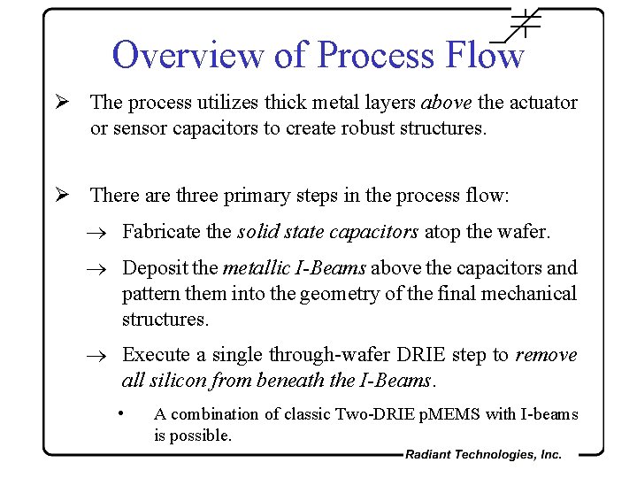
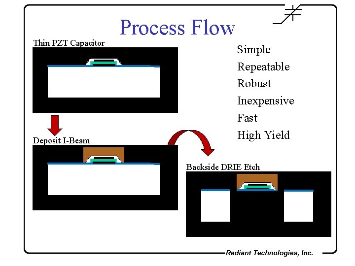
Overview of Process Flow Ø The process utilizes thick metal layers above the actuator or sensor capacitors to create robust structures. Ø There are three primary steps in the process flow: Fabricate the solid state capacitors atop the wafer. Deposit the metallic I-Beams above the capacitors and pattern them into the geometry of the final mechanical structures. Execute a single through-wafer DRIE step to remove all silicon from beneath the I-Beams. • Advanced Systems Test A combination of classic Two-DRIE p. MEMS with I-beams is possible.

Thin PZT Capacitor Deposit I-Beam Process Flow Simple Repeatable Robust Inexpensive Fast High Yield Backside DRIE Etch Advanced Systems Test

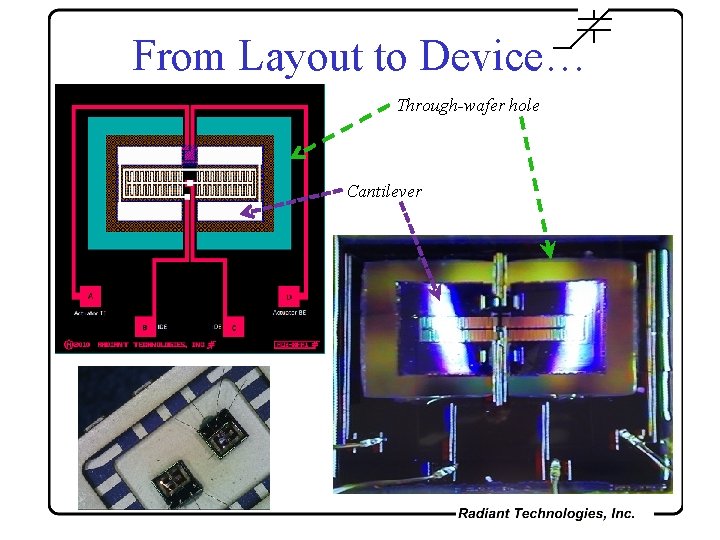
From Layout to Device… Through-wafer hole Cantilever Advanced Systems Test

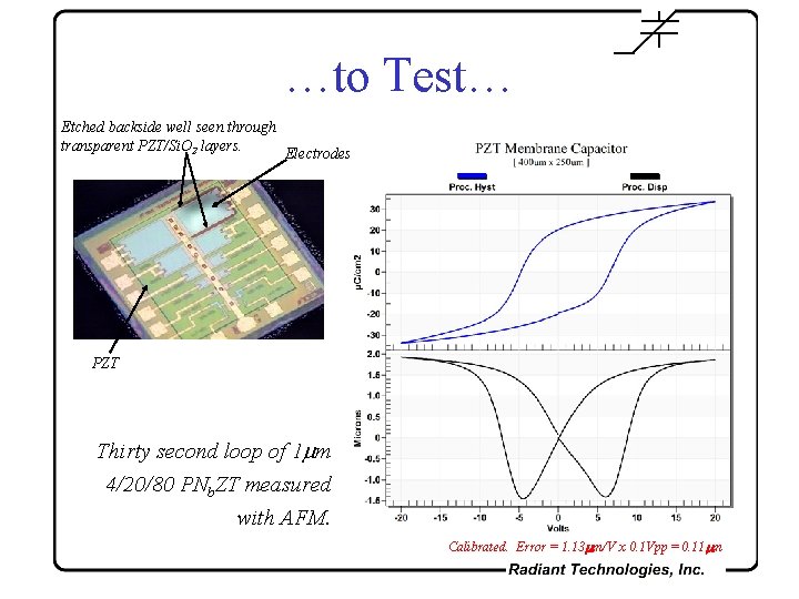
…to Test… Etched backside well seen through transparent PZT/Si. O 2 layers. Electrodes PZT Thirty second loop of 1 m 4/20/80 PNb. ZT measured with AFM. Calibrated. Error = 1. 13 m/V x 0. 1 Vpp = 0. 11 m Advanced Systems Test

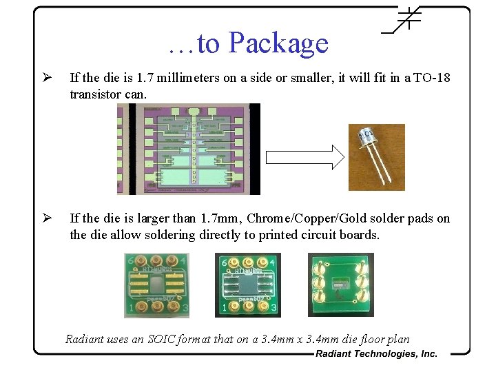
…to Package Ø If the die is 1. 7 millimeters on a side or smaller, it will fit in a TO-18 transistor can. Ø If the die is larger than 1. 7 mm, Chrome/Copper/Gold solder pads on the die allow soldering directly to printed circuit boards. Radiant uses an SOIC format that on a 3. 4 mm x 3. 4 mm die floor plan Advanced Systems Test

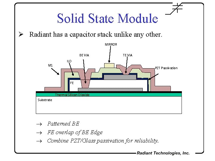
Solid State Module Ø Radiant has a capacitor stack unlike any other. MIRROR BE VIA M 1 TE VIA ILD PZT Passivation FE Thermal Silicon Dioxide Substrate Patterned BE FE overlap of BE Edge Combine PZT/Glass passivation for reliability. Advanced Systems Test

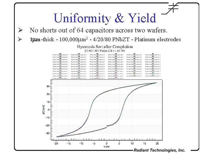
Uniformity & Yield Ø No shorts out of 64 capacitors across two wafers. Ø 1 m-thick - 100, 000 m 2 - 4/20/80 PNb. ZT - Platinum electrodes Advanced Systems Test

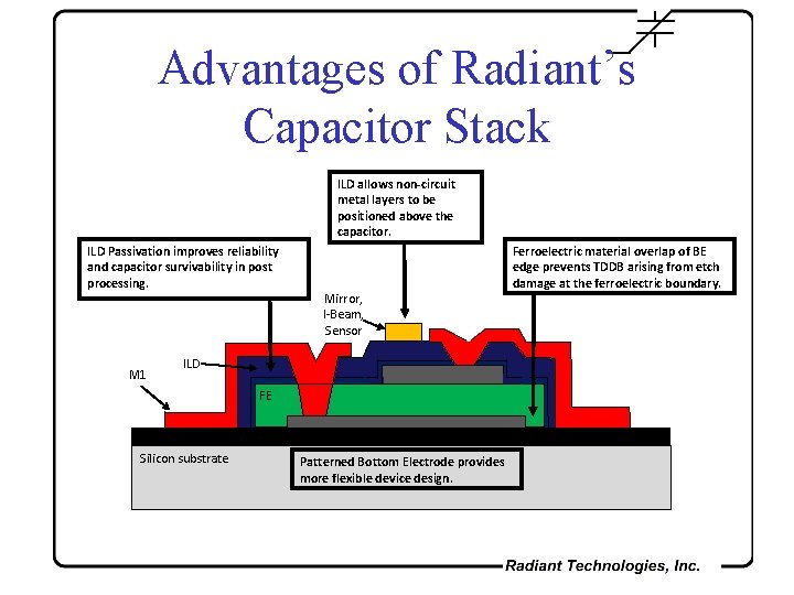
Advantages of Radiant’s Capacitor Stack ILD allows non-circuit metal layers to be positioned above the capacitor. ILD Passivation improves reliability and capacitor survivability in post processing. M 1 Mirror, I-Beam, Sensor ILD FE Silicon substrate Advanced Systems Test Patterned Bottom Electrode provides more flexible device design. Ferroelectric material overlap of BE edge prevents TDDB arising from etch damage at the ferroelectric boundary.

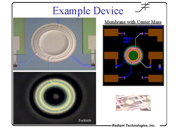
Example Device Membrane with Center Mass Backside Advanced Systems Test

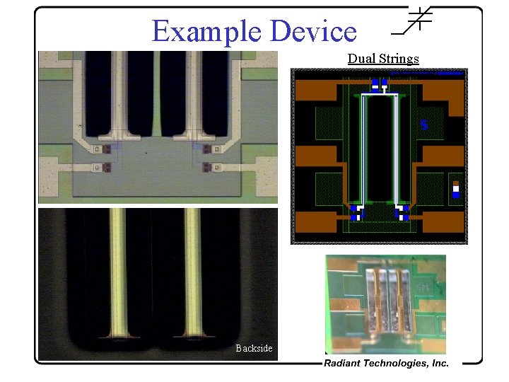
Example Device Dual Strings Backside Advanced Systems Test

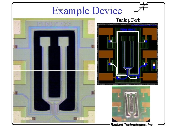
Example Device Tuning Fork Advanced Systems Test

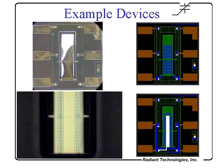
Example Devices Advanced Systems Test

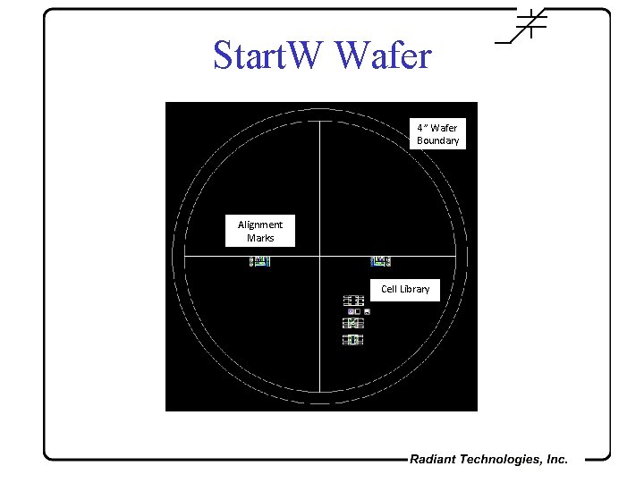
Project Flow Ø Radiant provides a GDS II file of the STARTW project. STARTW includes the wafer boundaries, alignment marks, and an assortment of design-rule-compliant cells such as vias, capacitors, solder pads, etc. that are building blocks for larger structures. Ø Radiant conducts a final design review of the project, acquire masks and fabricate the wafers. Ø Finished dice are be submitted to the researcher. Ø Radiant will advise on testing. Advanced Systems Test

Start. W Wafer 4” Wafer Boundary Alignment Marks Cell Library Advanced Systems Test

Contact Ø Please contact Naomi Montross or Joe Evans at Radiant Technologies in Albuquerque. +1 -505 -842 -8007 radiant@ferrodevices. com *** Ø This Power. Point file will be on-line at www. Ferro. Foundry. com Advanced Systems Test