Lecture 14 OUTLINE pn Junction Diodes contd Transient
- Slides: 17

Lecture 14 OUTLINE • pn Junction Diodes (cont’d) – Transient response: turn-on – Summary of important concepts – Diode applications • Varactor diodes • Tunnel diodes • Optoelectronic diodes Reading: Pierret 9; Hu 4. 12 -4. 15

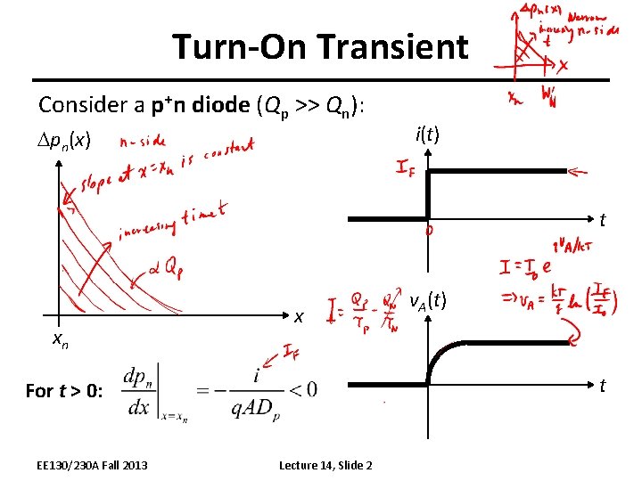
Turn-On Transient Consider a p+n diode (Qp >> Qn): Dpn(x) i(t) t xn x t For t > 0: EE 130/230 A Fall 2013 v. A(t) Lecture 14, Slide 2

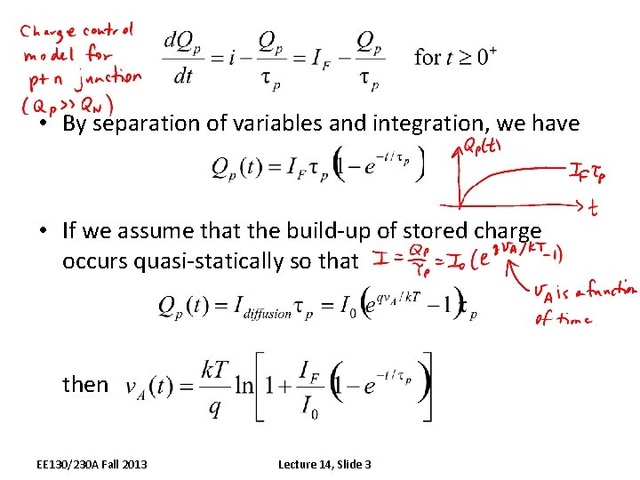
• By separation of variables and integration, we have • If we assume that the build-up of stored charge occurs quasi-statically so that then EE 130/230 A Fall 2013 Lecture 14, Slide 3

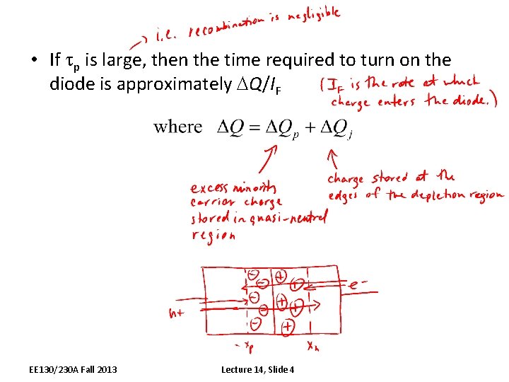
• If tp is large, then the time required to turn on the diode is approximately DQ/IF EE 130/230 A Fall 2013 Lecture 14, Slide 4

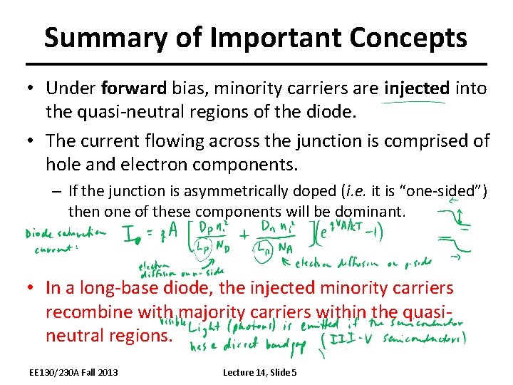
Summary of Important Concepts • Under forward bias, minority carriers are injected into the quasi-neutral regions of the diode. • The current flowing across the junction is comprised of hole and electron components. – If the junction is asymmetrically doped (i. e. it is “one-sided”) then one of these components will be dominant. • In a long-base diode, the injected minority carriers recombine with majority carriers within the quasineutral regions. EE 130/230 A Fall 2013 Lecture 14, Slide 5

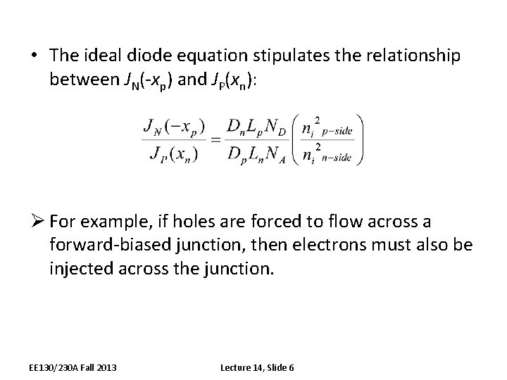
• The ideal diode equation stipulates the relationship between JN(-xp) and JP(xn): Ø For example, if holes are forced to flow across a forward-biased junction, then electrons must also be injected across the junction. EE 130/230 A Fall 2013 Lecture 14, Slide 6

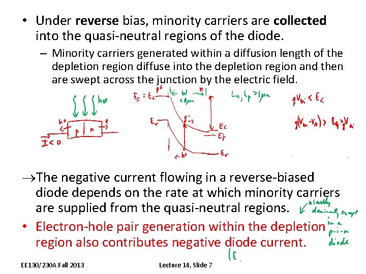
• Under reverse bias, minority carriers are collected into the quasi-neutral regions of the diode. – Minority carriers generated within a diffusion length of the depletion region diffuse into the depletion region and then are swept across the junction by the electric field. ®The negative current flowing in a reverse-biased diode depends on the rate at which minority carriers are supplied from the quasi-neutral regions. • Electron-hole pair generation within the depletion region also contributes negative diode current. EE 130/230 A Fall 2013 Lecture 14, Slide 7

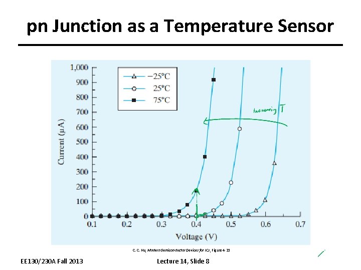
pn Junction as a Temperature Sensor C. C. Hu, Modern Semiconductor Devices for ICs, Figure 4 -21 EE 130/230 A Fall 2013 Lecture 14, Slide 8

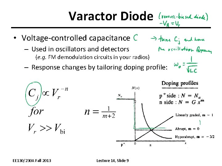
Varactor Diode • Voltage-controlled capacitance – Used in oscillators and detectors (e. g. FM demodulation circuits in your radios) – Response changes by tailoring doping profile: EE 130/230 A Fall 2013 Lecture 14, Slide 9

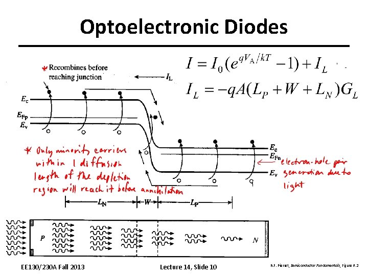
Optoelectronic Diodes EE 130/230 A Fall 2013 Lecture 14, Slide 10 R. F. Pierret, Semiconductor Fundamentals, Figure 9. 2

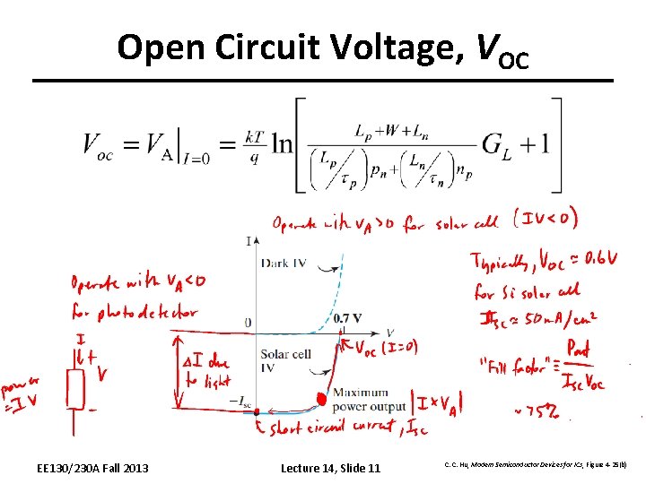
Open Circuit Voltage, VOC EE 130/230 A Fall 2013 Lecture 14, Slide 11 C. C. Hu, Modern Semiconductor Devices for ICs, Figure 4 -25(b)

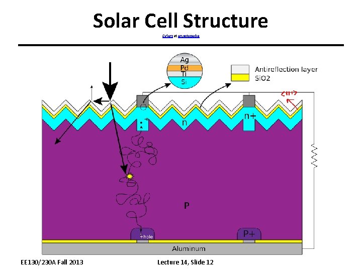
Solar Cell Structure Cyferz at en. wikipedia EE 130/230 A Fall 2013 Lecture 14, Slide 12

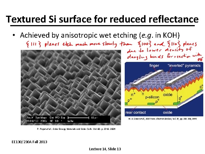
Textured Si surface for reduced reflectance • Achieved by anisotropic wet etching (e. g. in KOH) M. A. Green et al. , IEEE Trans. Electron Devices, Vol. 37, pp. 331 -336, 1990 P. Papet et al. , Solar Energy Materials and Solar Cells, Vol. 90, p. 2319, 2006 EE 130/230 A Fall 2013 Lecture 14, Slide 13

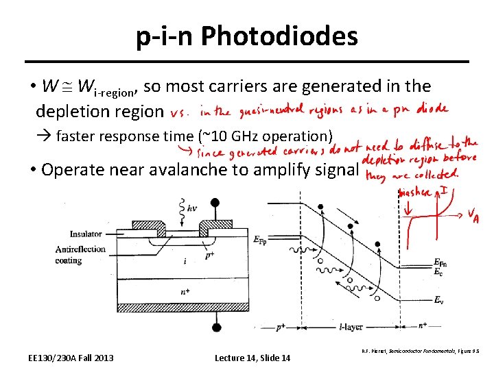
p-i-n Photodiodes • W Wi-region, so most carriers are generated in the depletion region faster response time (~10 GHz operation) • Operate near avalanche to amplify signal EE 130/230 A Fall 2013 Lecture 14, Slide 14 R. F. Pierret, Semiconductor Fundamentals, Figure 9. 5

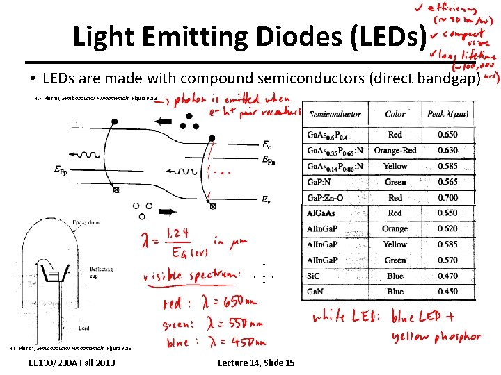
Light Emitting Diodes (LEDs) • LEDs are made with compound semiconductors (direct bandgap) R. F. Pierret, Semiconductor Fundamentals, Figure 9. 13 R. F. Pierret, Semiconductor Fundamentals, Figure 9. 15 EE 130/230 A Fall 2013 Lecture 14, Slide 15

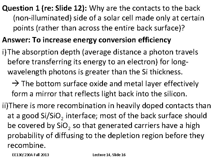
Question 1 (re: Slide 12): Why are the contacts to the back (non-illuminated) side of a solar cell made only at certain points (rather than across the entire back surface)? Answer: To increase energy conversion efficiency i) The absorption depth (average distance a photon travels before transferring its energy to an electron) for longwavelength photons is greater than the Si thickness. The bottom surface oxide and metal layer effectively form a mirror that reflects light back into the silicon. ii)There is more recombination in heavily doped contacts than at a good Si/Si. O 2 interface; most of the back surface should be covered by Si. O 2 so that generated carriers have a high probability of diffusing to the depletion region before they recombine. EE 130/230 A Fall 2013 Lecture 14, Slide 16

Question 2 (re: Slide 15): What limits the lifetime of an LED? Answer: i) LED lifetime is defined to be the duration of operation after which the light output falls to only 70% of original. (Even afterwards, the LED will continue to function. ) ii) The power density of an LED can be high (up to 10 W/cm 2, comparable to an electric stove top), causing significant heating which can degrade the light output through various mechanisms: 1. Degradation of epoxy package causing partial absorption of light 2. Mechanical stress weakening the wire bond (electrical connection) 3. Formation/growth of crystalline defects, or diffusion of metal into the semiconductor, resulting in increased recombination via midgap states EE 130/230 A Fall 2013 Lecture 14, Slide 17