Lecture 12 OUTLINE pn Junction Diodes contd Deviations
- Slides: 8

Lecture 12 OUTLINE • pn Junction Diodes (cont’d) – Deviations from the ideal I-V • R-G current • series resistance • high-level injection Reading: Pierret 6. 2

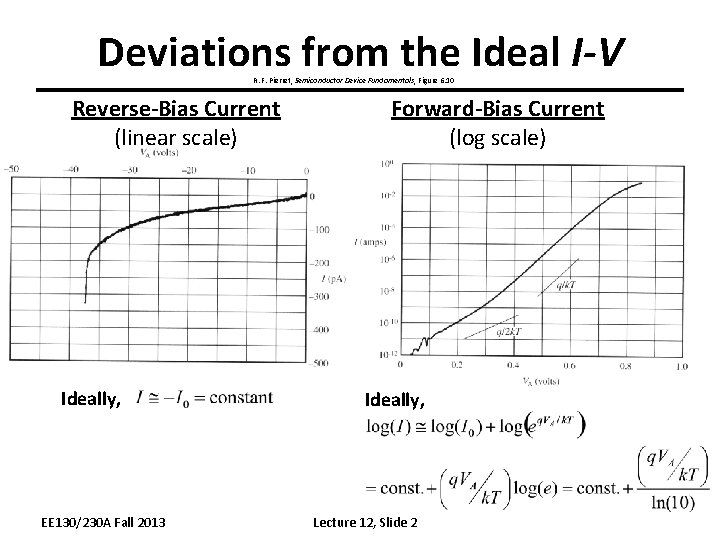
Deviations from the Ideal I-V R. F. Pierret, Semiconductor Device Fundamentals, Figure 6. 10 Reverse-Bias Current (linear scale) Ideally, EE 130/230 A Fall 2013 Forward-Bias Current (log scale) Ideally, Lecture 12, Slide 2

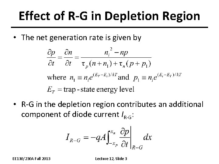
Effect of R-G in Depletion Region • The net generation rate is given by • R-G in the depletion region contributes an additional component of diode current IR-G: EE 130/230 A Fall 2013 Lecture 12, Slide 3

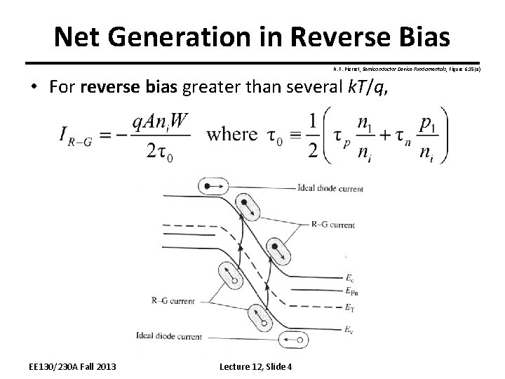
Net Generation in Reverse Bias R. F. Pierret, Semiconductor Device Fundamentals, Figure 6. 15(a) • For reverse bias greater than several k. T/q, EE 130/230 A Fall 2013 Lecture 12, Slide 4

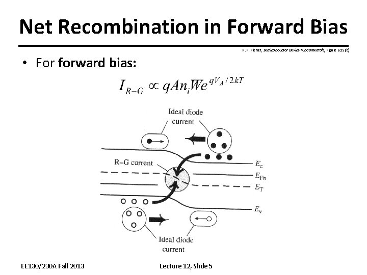
Net Recombination in Forward Bias R. F. Pierret, Semiconductor Device Fundamentals, Figure 6. 15(b) • For forward bias: EE 130/230 A Fall 2013 Lecture 12, Slide 5

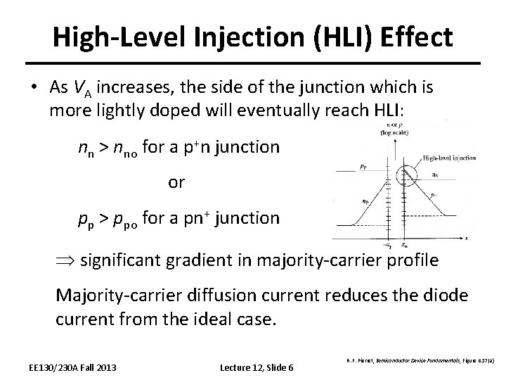
High-Level Injection (HLI) Effect • As VA increases, the side of the junction which is more lightly doped will eventually reach HLI: nn > nno for a p+n junction or pp > ppo for a pn+ junction Þ significant gradient in majority-carrier profile Majority-carrier diffusion current reduces the diode current from the ideal case. EE 130/230 A Fall 2013 Lecture 12, Slide 6 R. F. Pierret, Semiconductor Device Fundamentals, Figure 6. 17(a)

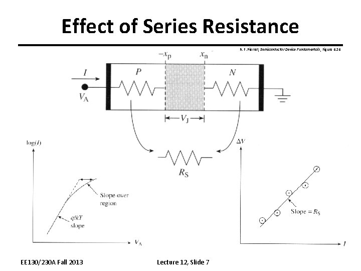
Effect of Series Resistance R. F. Pierret, Semiconductor Device Fundamentals, Figure 6. 16 EE 130/230 A Fall 2013 Lecture 12, Slide 7

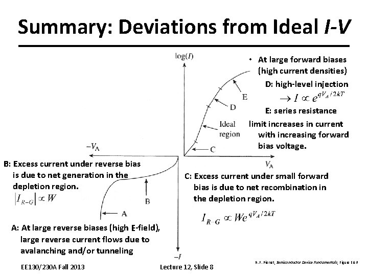
Summary: Deviations from Ideal I-V • At large forward biases (high current densities) D: high-level injection E: series resistance limit increases in current with increasing forward bias voltage. B: Excess current under reverse bias is due to net generation in the depletion region. C: Excess current under small forward bias is due to net recombination in the depletion region. A: At large reverse biases (high E-field), large reverse current flows due to avalanching and/or tunneling EE 130/230 A Fall 2013 Lecture 12, Slide 8 R. F. Pierret, Semiconductor Device Fundamentals, Figure E 6 -9