ENGIN 112 Intro to Electrical and Computer Engineering
- Slides: 16
ENGIN 112 Intro to Electrical and Computer Engineering Lecture 19 Sequential Circuits: Latches ENGIN 112 L 19: Sequential Circuits: Latches October 17, 2003
Overview ° Circuits require memory to store intermediate data ° Sequential circuits use a periodic signal to determine when to store values. • A clock signal can determine storage times • Clock signals are periodic ° Single bit storage element is a flip flop ° A basic type of flip flop is a latch ° Latches are made from logic gates • NAND, NOR, AND, OR, Inverter ENGIN 112 L 19: Sequential Circuits: Latches October 17, 2003
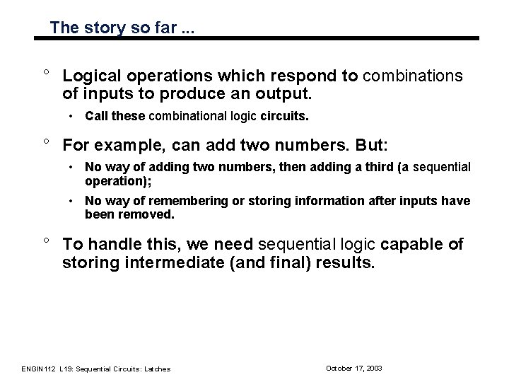
The story so far. . . ° Logical operations which respond to combinations of inputs to produce an output. • Call these combinational logic circuits. ° For example, can add two numbers. But: • No way of adding two numbers, then adding a third (a sequential operation); • No way of remembering or storing information after inputs have been removed. ° To handle this, we need sequential logic capable of storing intermediate (and final) results. ENGIN 112 L 19: Sequential Circuits: Latches October 17, 2003
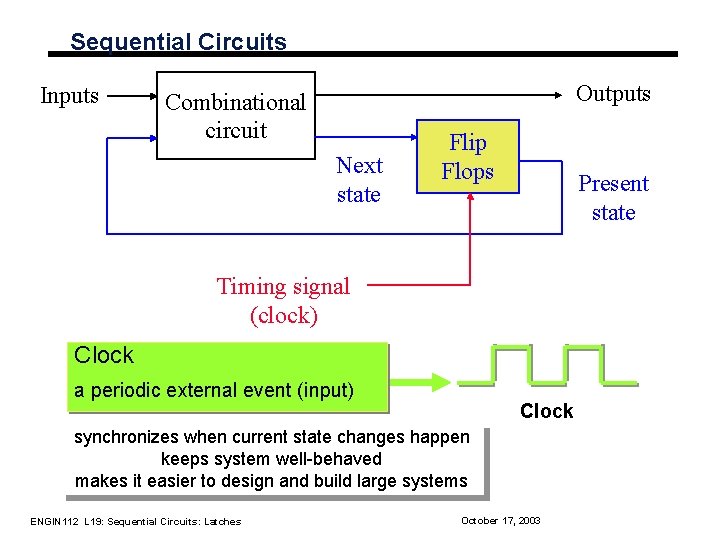
Sequential Circuits Inputs Outputs Combinational circuit Next state Flip Flops Present state Timing signal (clock) Clock a periodic external event (input) Clock synchronizes when current state changes happen keeps system well-behaved makes it easier to design and build large systems ENGIN 112 L 19: Sequential Circuits: Latches October 17, 2003
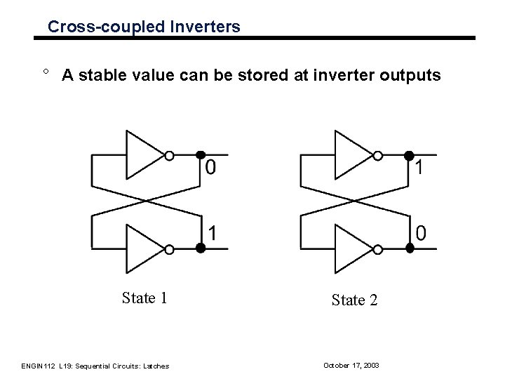
Cross-coupled Inverters ° A stable value can be stored at inverter outputs State 1 State 2 ENGIN 112 L 19: Sequential Circuits: Latches October 17, 2003
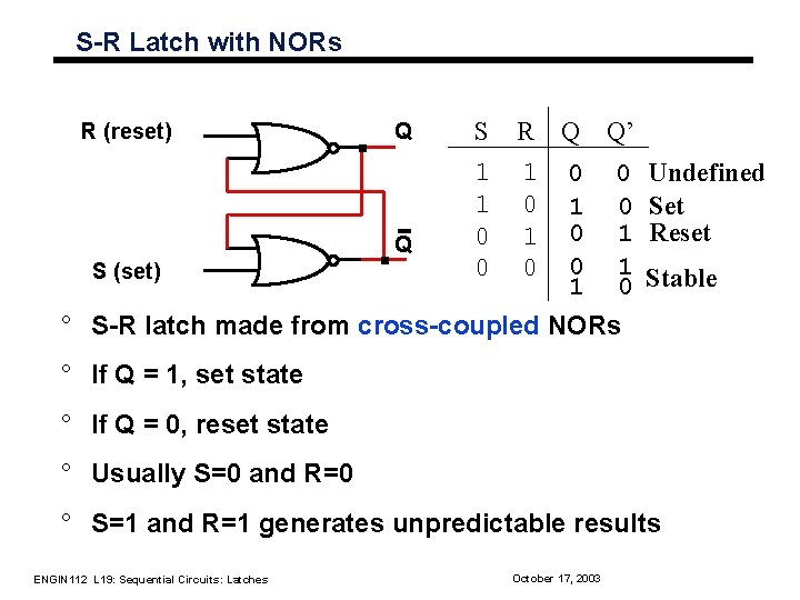
S-R Latch with NORs S R Q Q’ 1 1 0 0 1 0 1 Q 0 0 0 1 S (set) 1 0 ° S-R latch made from cross-coupled NORs R (reset) Q Undefined Set Reset Stable ° If Q = 1, set state ° If Q = 0, reset state ° Usually S=0 and R=0 ° S=1 and R=1 generates unpredictable results ENGIN 112 L 19: Sequential Circuits: Latches October 17, 2003
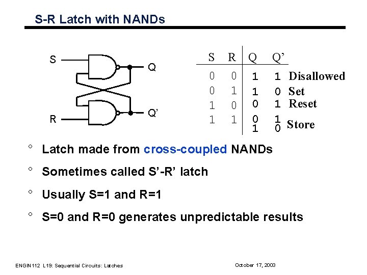
S-R Latch with NANDs S R Q Q’ S R Q 0 0 1 1 1 0 0 1 1 0 1 Q’ 1 0 1 1 0 Disallowed Set Reset Store ° Latch made from cross-coupled NANDs ° Sometimes called S’-R’ latch ° Usually S=1 and R=1 ° S=0 and R=0 generates unpredictable results ENGIN 112 L 19: Sequential Circuits: Latches October 17, 2003
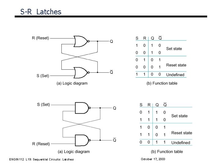
S-R Latches ENGIN 112 L 19: Sequential Circuits: Latches October 17, 2003
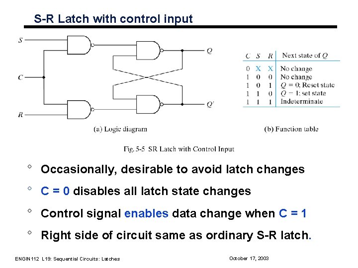
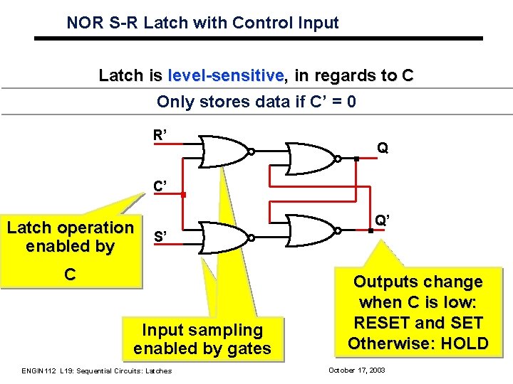
S-R Latch with control input ° Occasionally, desirable to avoid latch changes ° C = 0 disables all latch state changes ° Control signal enables data change when C = 1 ° Right side of circuit same as ordinary S-R latch. ENGIN 112 L 19: Sequential Circuits: Latches October 17, 2003
NOR S-R Latch with Control Input Latch is level-sensitive, in regards to C Only stores data if C’ = 0 R’ Q C’ Latch operation enabled by Q’ S’ C Input sampling enabled by gates ENGIN 112 L 19: Sequential Circuits: Latches Outputs change when C is low: RESET and SET Otherwise: HOLD October 17, 2003
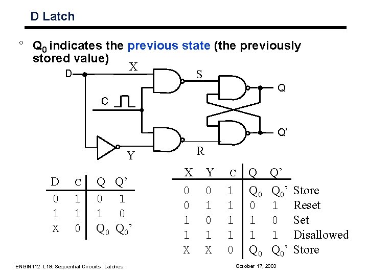
D Latch ° Q 0 indicates the previous state (the previously stored value) X D S Q C Q’ R Y D 0 1 X C 1 1 0 Q 0 1 Q 0 Q’ 1 0 Q 0’ ENGIN 112 L 19: Sequential Circuits: Latches X 0 0 1 1 X Y 0 1 X C 1 1 0 Q Q 0 0 1 1 Q 0 Q’ Q 0’ 1 0 1 Q 0’ October 17, 2003 Store Reset Set Disallowed Store
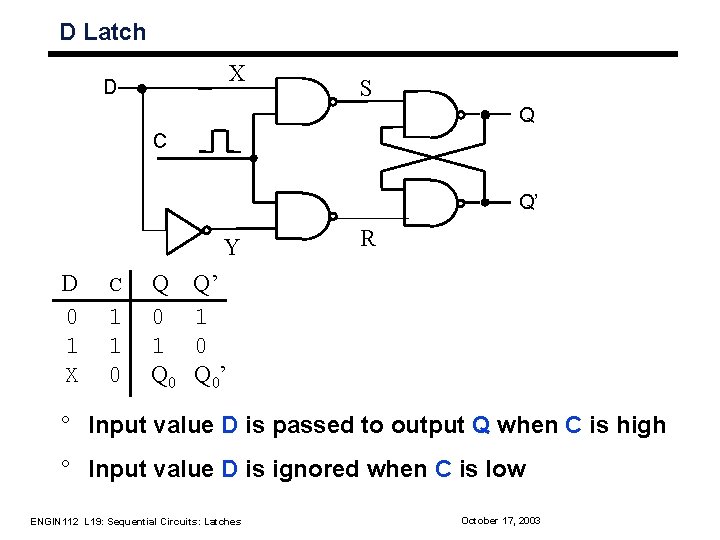
D Latch X D S Q C Q’ Y D 0 1 X C 1 1 0 Q 0 1 Q 0 R Q’ 1 0 Q 0’ ° Input value D is passed to output Q when C is high ° Input value D is ignored when C is low ENGIN 112 L 19: Sequential Circuits: Latches October 17, 2003
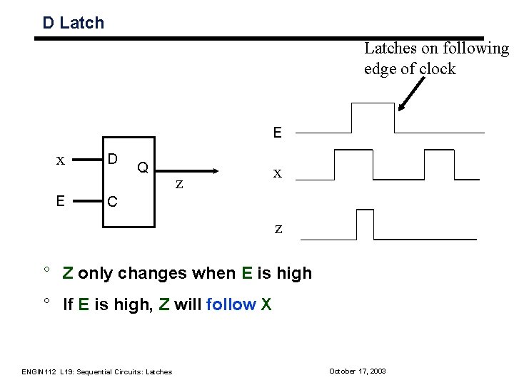
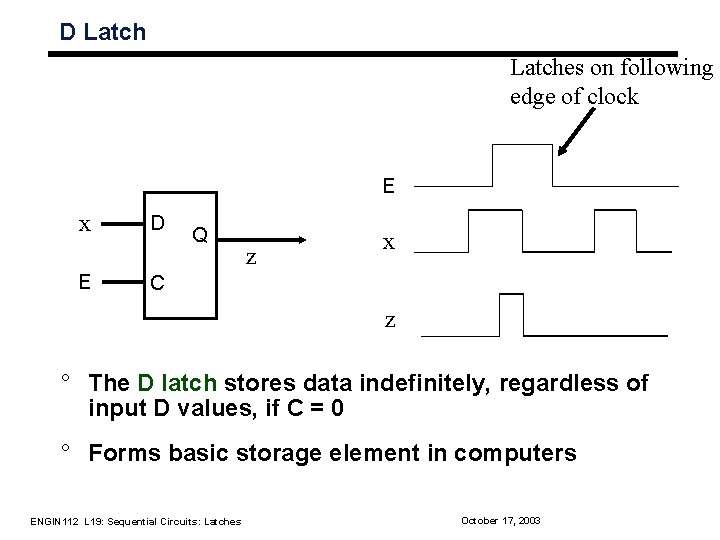
D Latches on following edge of clock E x E D Q z x C z ° Z only changes when E is high ° If E is high, Z will follow X ENGIN 112 L 19: Sequential Circuits: Latches October 17, 2003
D Latches on following edge of clock E x E D Q z x C z ° The D latch stores data indefinitely, regardless of input D values, if C = 0 ° Forms basic storage element in computers ENGIN 112 L 19: Sequential Circuits: Latches October 17, 2003
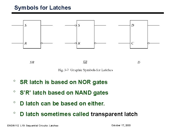
Symbols for Latches ° SR latch is based on NOR gates ° S’R’ latch based on NAND gates ° D latch can be based on either. ° D latch sometimes called transparent latch ENGIN 112 L 19: Sequential Circuits: Latches October 17, 2003
Summary ° Latches are based on combinational gates (e. g. NAND, NOR) ° Latches store data even after data input has been removed ° S-R latches operate like cross-coupled inverters with control inputs (S = set, R = reset) ° With additional gates, an S-R latch can be converted to a D latch (D stands for data) ° D latch is simple to understand conceptually • When C = 1, data input D stored in latch and output as Q • When C = 0, data input D ignored and previous latch value output at Q ° Next time: more storage elements! ENGIN 112 L 19: Sequential Circuits: Latches October 17, 2003