EE 130230 A Discussion 11 Peng Zheng 1


- Slides: 11
EE 130/230 A Discussion 11 Peng Zheng 1
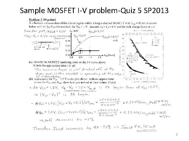
Sample MOSFET I-V problem-Quiz 5 SP 2013 2
Sample MOSFET I-V problem-Quiz 5 SP 2013 3
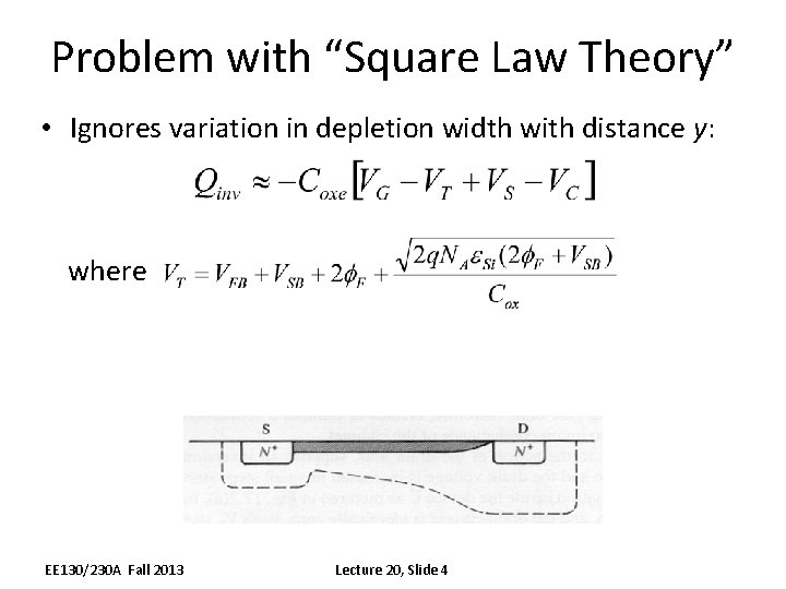
Problem with “Square Law Theory” • Ignores variation in depletion width with distance y: where EE 130/230 A Fall 2013 Lecture 20, Slide 4
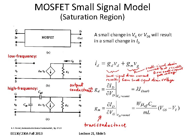
MOSFET Small Signal Model (Saturation Region) • Conductance parameters: A small change in VG or VDS will result in a small change in ID low-frequency: high-frequency: R. F. Pierret, Semiconductor Device Fundamentals, Fig. 17. 12 EE 130/230 A Fall 2013 Lecture 21, Slide 5
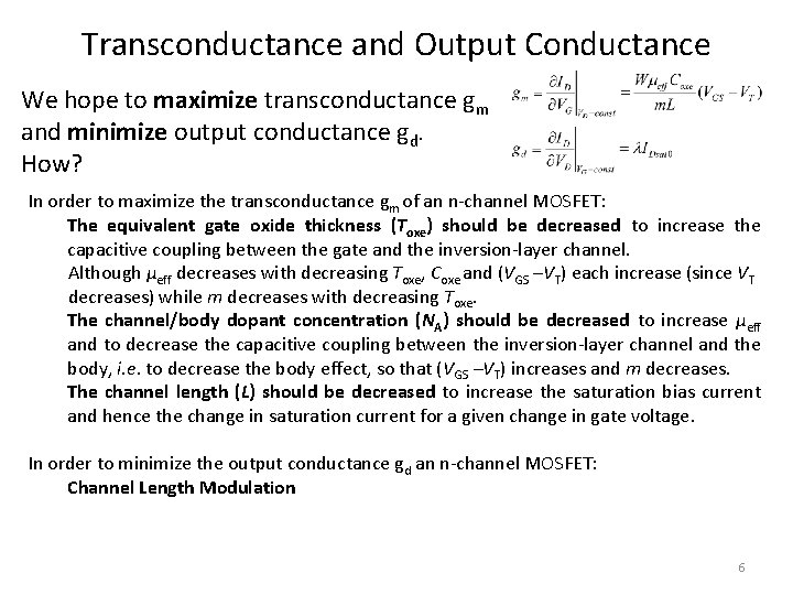
Transconductance and Output Conductance We hope to maximize transconductance gm and minimize output conductance gd. How? In order to maximize the transconductance gm of an n-channel MOSFET: The equivalent gate oxide thickness (Toxe) should be decreased to increase the capacitive coupling between the gate and the inversion-layer channel. Although µeff decreases with decreasing Toxe, Coxe and (VGS –VT) each increase (since VT decreases) while m decreases with decreasing Toxe. The channel/body dopant concentration (NA) should be decreased to increase µeff and to decrease the capacitive coupling between the inversion-layer channel and the body, i. e. to decrease the body effect, so that (VGS –VT) increases and m decreases. The channel length (L) should be decreased to increase the saturation bias current and hence the change in saturation current for a given change in gate voltage. In order to minimize the output conductance gd an n-channel MOSFET: Channel Length Modulation 6
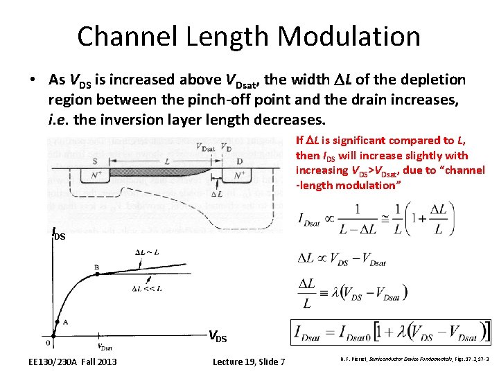
Channel Length Modulation • As VDS is increased above VDsat, the width DL of the depletion region between the pinch-off point and the drain increases, i. e. the inversion layer length decreases. If DL is significant compared to L, then IDS will increase slightly with increasing VDS>VDsat, due to “channel -length modulation” IDS VDS EE 130/230 A Fall 2013 Lecture 19, Slide 7 R. F. Pierret, Semiconductor Device Fundamentals, Figs. 17. 2, 17 -3
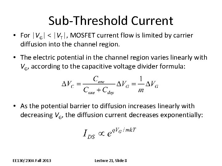
Sub-Threshold Current • For |VG| < |VT|, MOSFET current flow is limited by carrier diffusion into the channel region. • The electric potential in the channel region varies linearly with VG, according to the capacitive voltage divider formula: • As the potential barrier to diffusion increases linearly with decreasing VG, the diffusion current decreases exponentially: EE 130/230 A Fall 2013 Lecture 21, Slide 8
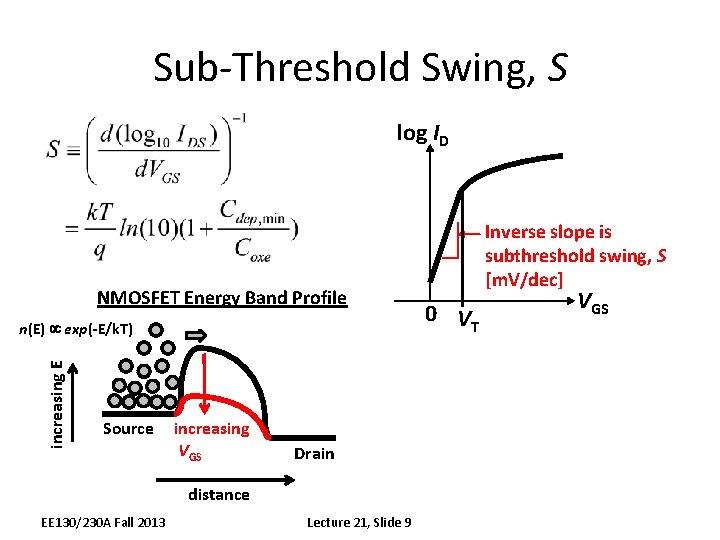
Sub-Threshold Swing, S log ID NMOSFET Energy Band Profile increasing E n(E) exp(-E/k. T) Source increasing VGS Drain distance EE 130/230 A Fall 2013 Lecture 21, Slide 9 Inverse slope is subthreshold swing, S [m. V/dec] 0 VT VGS
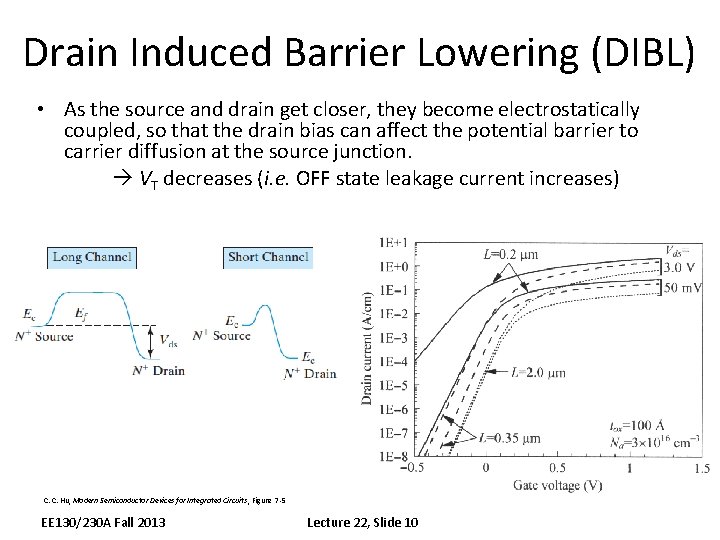
Drain Induced Barrier Lowering (DIBL) • As the source and drain get closer, they become electrostatically coupled, so that the drain bias can affect the potential barrier to carrier diffusion at the source junction. VT decreases (i. e. OFF state leakage current increases) C. C. Hu, Modern Semiconductor Devices for Integrated Circuits, Figure 7 -5 EE 130/230 A Fall 2013 Lecture 22, Slide 10
Questions regarding project? Good luck to Quiz#5! 11