Design and Implementation of VLSI Systems EN 1600

- Slides: 10
Design and Implementation of VLSI Systems (EN 1600) Lecture 17: Design Considerations Prof. Sherief Reda Division of Engineering, Brown University Spring 2008 [sources: Weste/Addison Wesley – Rabaey/Pearson] S. Reda EN 160 SP’ 08
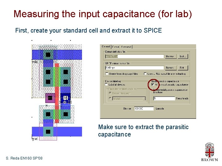
Measuring the input capacitance (for lab) First, create your standard cell and extract it to SPICE Make sure to extract the parasitic capacitance S. Reda EN 160 SP’ 08
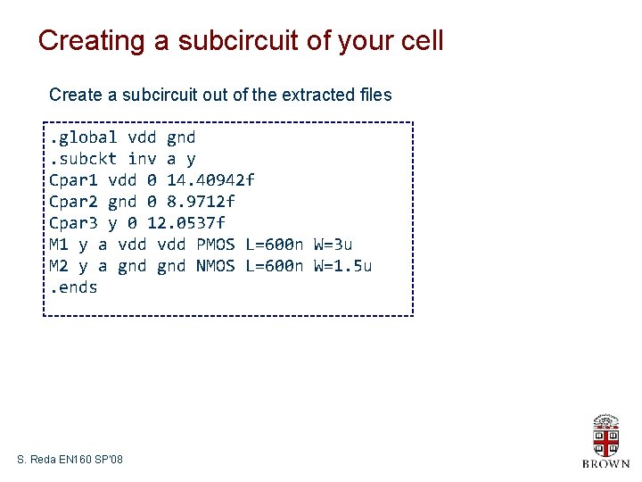
Creating a subcircuit of your cell Create a subcircuit out of the extracted files. global vdd gnd. subckt inv a y Cpar 1 vdd 0 14. 40942 f Cpar 2 gnd 0 8. 9712 f Cpar 3 y 0 12. 0537 f M 1 y a vdd PMOS L=600 n W=3 u M 2 y a gnd NMOS L=600 n W=1. 5 u. ends S. Reda EN 160 SP’ 08
Basic idea c I 3 CAP I 2 I 1 a delay of I 1 y f • Delay from a to y depend on the load capacitance of I 1 → input capacitance of I 2 • If CAP has the same capacitance as I 2 then delay from a to c will be equal to delay from a to y • Objective: try to “guess” CAP to equalize the delay S. Reda EN 160 SP’ 08
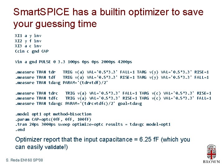
Smart. SPICE has a builtin optimizer to save your guessing time XI 1 a y inv XI 2 y f inv XI 3 a c inv Ccin c gnd CAP Vin a gnd PULSE 0 3. 3 100 ps 0 ps 2000 ps 4200 ps. measure TRAN tdr TRIG v(a) VAL='0. 5*3. 3' FALL=1 TARG v(y) VAL='0. 5*3. 3' RISE=1. measure TRAN tdf TRIG v(a) VAL='0. 5*3. 3' RISE=1 TARG v(y) VAL='0. 5*3. 3' FALL=1. measure TRAN tdavg PARAM='(tdr+tdf)/2'. measure TRAN tdrc TRIG v(a) VAL='0. 5*3. 3' FALL=1 TARG v(c) VAL='0. 5*3. 3' RISE=1. measure TRAN tdfc TRIG v(a) VAL='0. 5*3. 3' RISE=1 TARG v(c) VAL='0. 5*3. 3' FALL=1. measure TRAN tdavgc PARAM='(tdrc+tdfc)/2' goal=tdavg. model opt 1 opt method=bisection. param CAP=optc(0 f. F, 100 f. F). tran 20 ps 3000 ps sweep optimize=optc results = tdavgc model=opt 1. end Optimizer report that the input capacitance = 6. 25 f. F (which you can easily validate!) S. Reda EN 160 SP’ 08
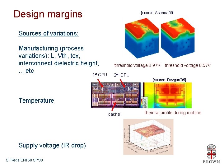
Design margins [source: Asenov’ 99] Sources of variations: Manufacturing (process variations): L, Vth, tox, interconnect dielectric height, . . , etc st 1 CPU threshold voltage 0. 97 V threshold voltage 0. 57 V 2 nd CPU [source: Devgan’ 05] Temperature cache Supply voltage (IR drop) S. Reda EN 160 SP’ 08 thermal profile during runtime
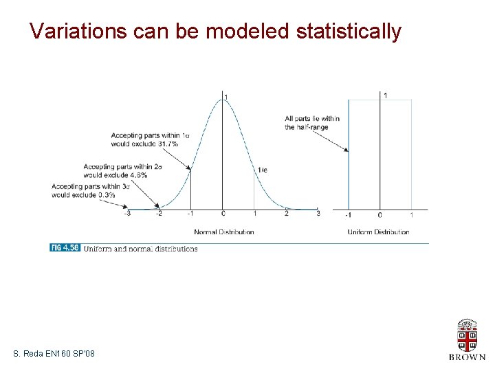
Variations can be modeled statistically S. Reda EN 160 SP’ 08
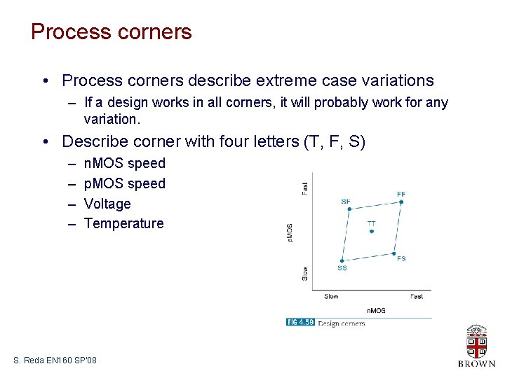
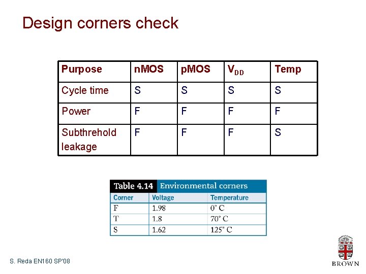
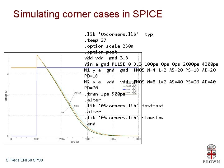
Process corners • Process corners describe extreme case variations – If a design works in all corners, it will probably work for any variation. • Describe corner with four letters (T, F, S) – – n. MOS speed p. MOS speed Voltage Temperature S. Reda EN 160 SP’ 08
Design corners check Purpose n. MOS p. MOS VDD Temp Cycle time S S Power F F Subthrehold leakage F F F S S. Reda EN 160 SP’ 08
Simulating corner cases in SPICE. lib '05 corners. lib' typ. temp 27. option scale=250 n. option post vdd gnd 3. 3 Vin a gnd PULSE 0 3. 3 100 ps 0 ps 2000 ps 4200 ps M 1 y a gnd NMOS W=4 L=2 AS=20 PS=18 AD=20 PD=18 M 2 y a vdd PMOS W=8 L=2 AS=40 PS=26 AD=40 PD=26. tran 1 ps 500 ps. alter. lib '05 corners. lib' fast. alter. lib '05 corners. lib' slow. end S. Reda EN 160 SP’ 08