Compact DSM MOS Modeling for EnergyDelay Estimation Joshua
- Slides: 10

Compact DSM MOS Modeling for Energy/Delay Estimation Joshua Garrett, Dr. Borivoje Nikolic Joshua L. Garrett Digital Circuits Design Group University of California, Berkeley

Abstract Increasingly, designers rely on SPICE simulation as the first serious entry point for circuit design, since commonly used models do not capture many important short channel device effects. This work focuses on development of compact device models which properly account for these effects, while remaining simple enough for “back of the envelope” calculations. These models are further developed as the basis for a static timing framework with maintains explicit supply and threshold dependence, and allow for first-order device variation calculations from a nominal set of I-V curves. Joshua L. Garrett Digital Circuits Design Group University of California, Berkeley

Accurate Compact Models • • • Aggressive energy-delay tradeoff techniques require accurate modeling on many levels: – Circuit level (load capacitance, input transition time) – Gate level (transistor equivalent resistance, parasitic capacitance, logical effort) – Device level (diffusion currents, mobility degradation, velocity saturation, DIBL) Compact models make parameter extraction tractable without in-depth knowledge of process Intuition based on hand calculation can greatly decrease design time Joshua L. Garrett Digital Circuits Design Group University of California, Berkeley

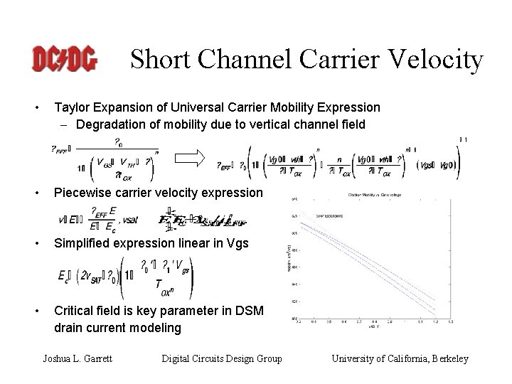
Short Channel Carrier Velocity • Taylor Expansion of Universal Carrier Mobility Expression – Degradation of mobility due to vertical channel field • Piecewise carrier velocity expression • Simplified expression linear in Vgs • Critical field is key parameter in DSM drain current modeling Joshua L. Garrett Digital Circuits Design Group University of California, Berkeley

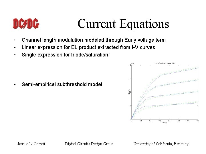
Current Equations • • • Channel length modulation modeled through Early voltage term Linear expression for EL product extracted from I-V curves Single expression for triode/saturation* • Semi-empirical subthreshold model Joshua L. Garrett Digital Circuits Design Group University of California, Berkeley

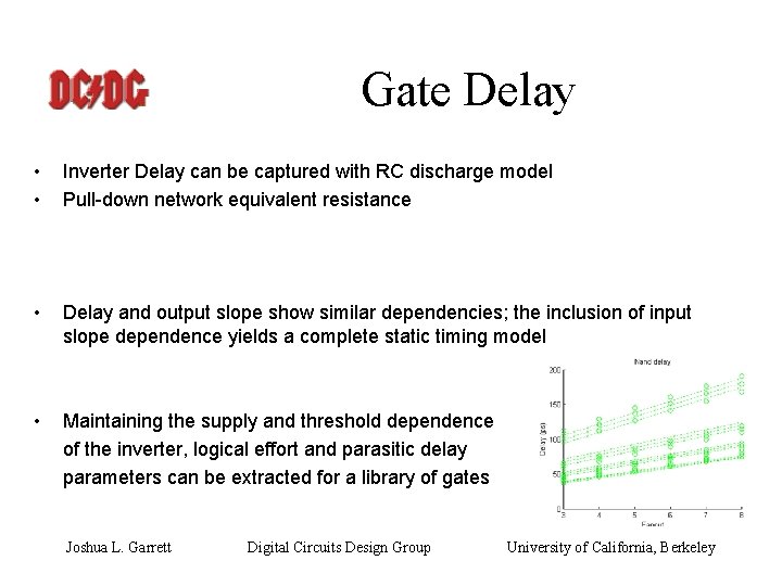
Gate Delay • • Inverter Delay can be captured with RC discharge model Pull-down network equivalent resistance • Delay and output slope show similar dependencies; the inclusion of input slope dependence yields a complete static timing model • Maintaining the supply and threshold dependence of the inverter, logical effort and parasitic delay parameters can be extracted for a library of gates Joshua L. Garrett Digital Circuits Design Group University of California, Berkeley

Device Variability • • Form of current models yields first-order expressions for device variability Major components of drain current mismatch (vth, tox, L, W, VDD) – Includes short channel effects, but not narrow width • Variation due to threshold, oxide thickness, gate length, and supply Joshua L. Garrett Digital Circuits Design Group University of California, Berkeley

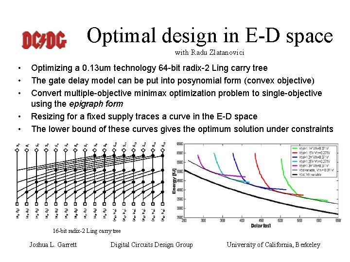
Optimal design in E-D space with Radu Zlatanovici • • • Optimizing a 0. 13 um technology 64 -bit radix-2 Ling carry tree The gate delay model can be put into posynomial form (convex objective) Convert multiple-objective minimax optimization problem to single-objective using the epigraph form Resizing for a fixed supply traces a curve in the E-D space The lower bound of these curves gives the optimum solution under constraints 16 -bit radix-2 Ling carry tree Joshua L. Garrett Digital Circuits Design Group University of California, Berkeley

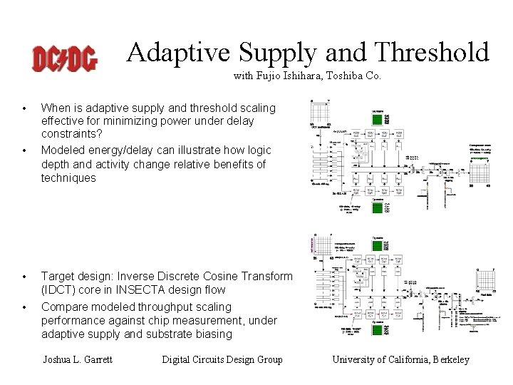
Adaptive Supply and Threshold with Fujio Ishihara, Toshiba Co. • • When is adaptive supply and threshold scaling effective for minimizing power under delay constraints? Modeled energy/delay can illustrate how logic depth and activity change relative benefits of techniques Target design: Inverse Discrete Cosine Transform (IDCT) core in INSECTA design flow Compare modeled throughput scaling performance against chip measurement, under adaptive supply and substrate biasing Joshua L. Garrett Digital Circuits Design Group University of California, Berkeley

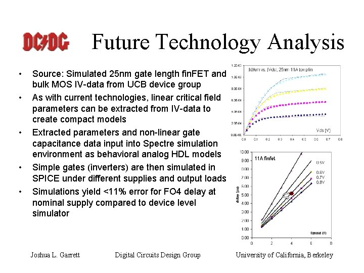
Future Technology Analysis • • • Source: Simulated 25 nm gate length fin. FET and bulk MOS IV-data from UCB device group As with current technologies, linear critical field parameters can be extracted from IV-data to create compact models Extracted parameters and non-linear gate capacitance data input into Spectre simulation environment as behavioral analog HDL models Simple gates (inverters) are then simulated in SPICE under different supplies and output loads Simulations yield <11% error for FO 4 delay at nominal supply compared to device level simulator Joshua L. Garrett Digital Circuits Design Group University of California, Berkeley