CIS 6930 Chip Multiprocessor Parallel Architecture and Programming
- Slides: 17

CIS 6930: Chip Multiprocessor: Parallel Architecture and Programming Fall 2009 Jih-Kwon Peir Computer Information Science Engineering University of Florida 1

Chapter 12: Fermi – New NVIDIA GPU Architecture o http: //www. pcper. com/article. php? aid=789 o http: //www. nvidia. com/object/fermi_architecture. html o http: //www. nvidia. com/content/PDF/fermi_white_papers/P. Glask owsky_NVIDIA's_Fermi. The_First_Complete_GPU_Architecture. pdf o http: //techreport. com/articles. x/17670/3 2

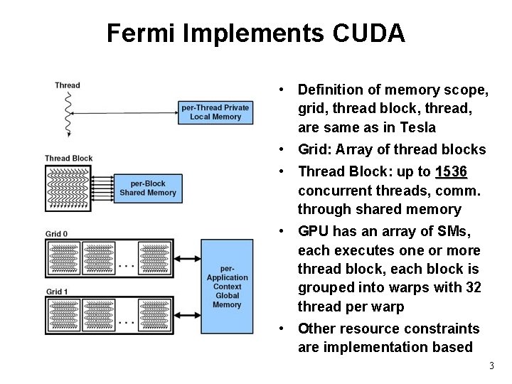
Fermi Implements CUDA • Definition of memory scope, grid, thread block, thread, are same as in Tesla • Grid: Array of thread blocks • Thread Block: up to 1536 concurrent threads, comm. through shared memory • GPU has an array of SMs, each executes one or more thread block, each block is grouped into warps with 32 thread per warp • Other resource constraints are implementation based 3

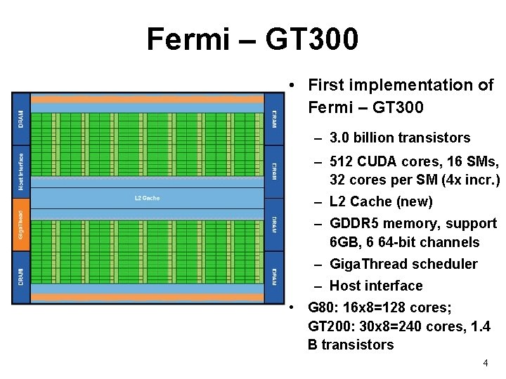
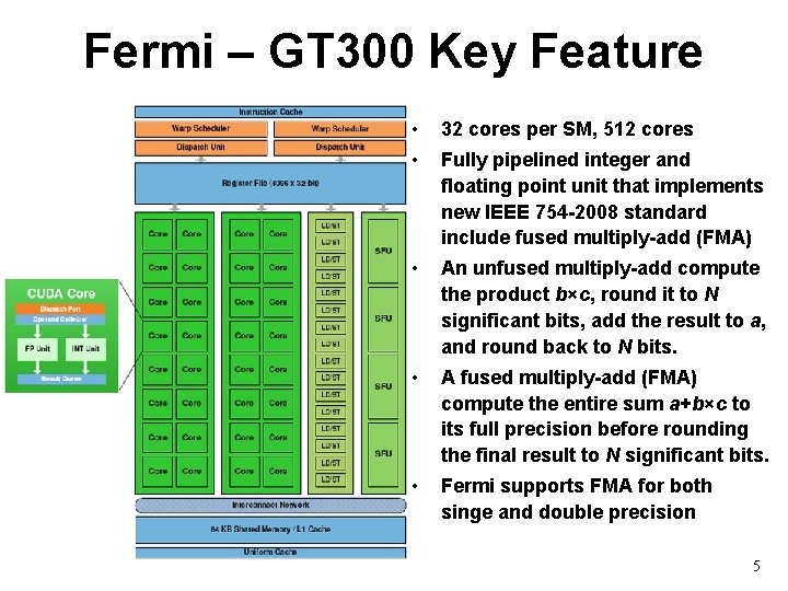
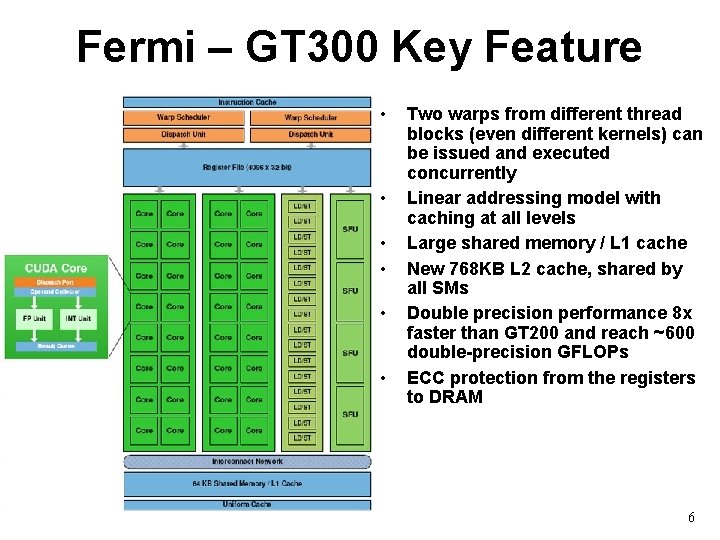
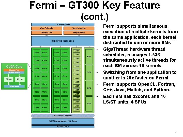
Fermi – GT 300 • First implementation of Fermi – GT 300 – 3. 0 billion transistors – 512 CUDA cores, 16 SMs, 32 cores per SM (4 x incr. ) – L 2 Cache (new) – GDDR 5 memory, support 6 GB, 6 64 -bit channels – Giga. Thread scheduler – Host interface • G 80: 16 x 8=128 cores; GT 200: 30 x 8=240 cores, 1. 4 B transistors 4

Fermi – GT 300 Key Feature • 32 cores per SM, 512 cores • Fully pipelined integer and floating point unit that implements new IEEE 754 -2008 standard include fused multiply-add (FMA) • An unfused multiply-add compute the product b×c, round it to N significant bits, add the result to a, and round back to N bits. • A fused multiply-add (FMA) compute the entire sum a+b×c to its full precision before rounding the final result to N significant bits. • Fermi supports FMA for both singe and double precision 5

Fermi – GT 300 Key Feature • • • Two warps from different thread blocks (even different kernels) can be issued and executed concurrently Linear addressing model with caching at all levels Large shared memory / L 1 cache New 768 KB L 2 cache, shared by all SMs Double precision performance 8 x faster than GT 200 and reach ~600 double-precision GFLOPs ECC protection from the registers to DRAM 6

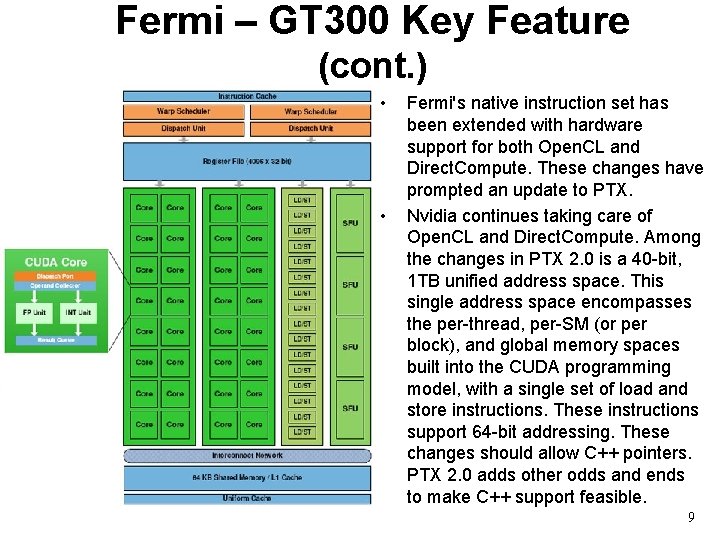
Fermi – GT 300 Key Feature (cont. ) • • • Fermi supports simultaneous execution of multiple kernels from the same application, each kernel distributed to one or more SMs Giga. Thread hardware thread scheduler, manages 1, 536 simultaneously active threads for each SM across 16 kernels Switching from one application to another is 20 x faster on Fermi supports Open. CL, Fortran, C++, Java, Matlab, and Python. Each SM has 32 cores and 16 LS/ST units, 4 SFUs 7

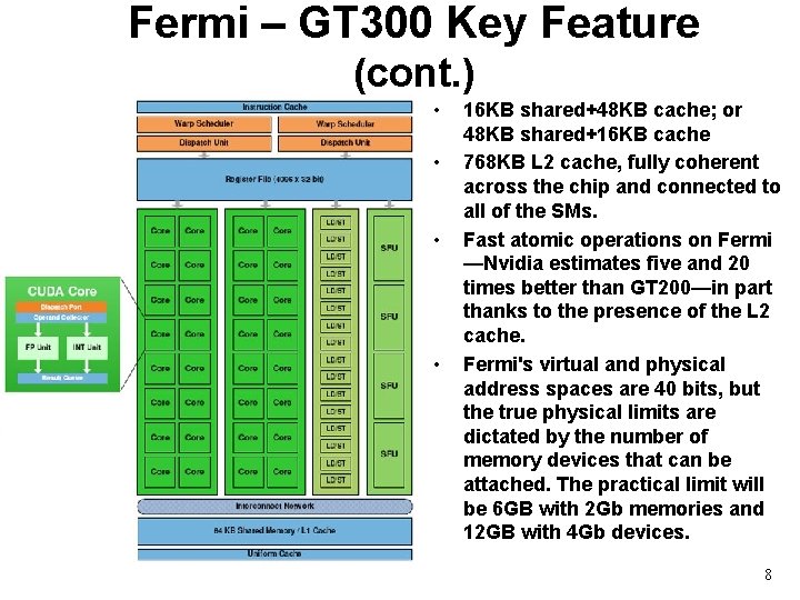
Fermi – GT 300 Key Feature (cont. ) • • 16 KB shared+48 KB cache; or 48 KB shared+16 KB cache 768 KB L 2 cache, fully coherent across the chip and connected to all of the SMs. Fast atomic operations on Fermi —Nvidia estimates five and 20 times better than GT 200—in part thanks to the presence of the L 2 cache. Fermi's virtual and physical address spaces are 40 bits, but the true physical limits are dictated by the number of memory devices that can be attached. The practical limit will be 6 GB with 2 Gb memories and 12 GB with 4 Gb devices. 8

Fermi – GT 300 Key Feature (cont. ) • • Fermi's native instruction set has been extended with hardware support for both Open. CL and Direct. Compute. These changes have prompted an update to PTX. Nvidia continues taking care of Open. CL and Direct. Compute. Among the changes in PTX 2. 0 is a 40 -bit, 1 TB unified address space. This single address space encompasses the per-thread, per-SM (or per block), and global memory spaces built into the CUDA programming model, with a single set of load and store instructions. These instructions support 64 -bit addressing. These changes should allow C++ pointers. PTX 2. 0 adds other odds and ends to make C++ support feasible. 9

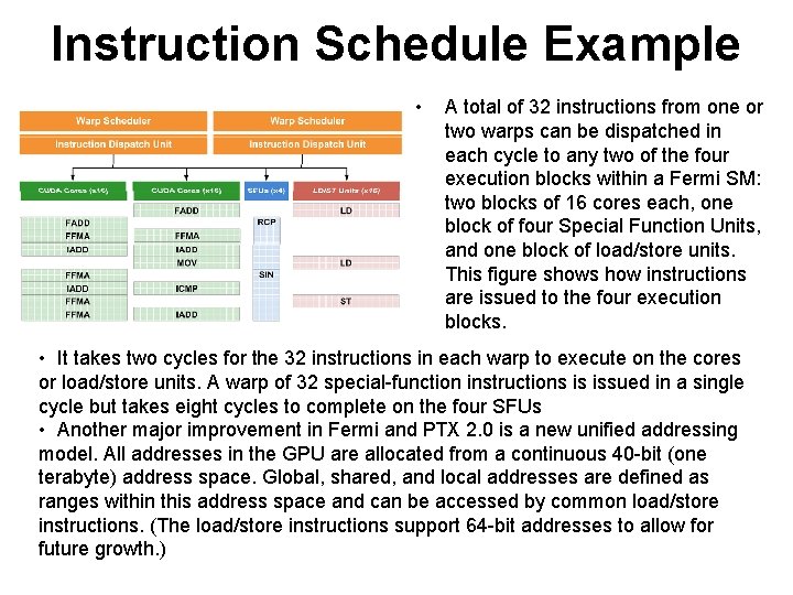
Instruction Schedule Example • A total of 32 instructions from one or two warps can be dispatched in each cycle to any two of the four execution blocks within a Fermi SM: two blocks of 16 cores each, one block of four Special Function Units, and one block of load/store units. This figure shows how instructions are issued to the four execution blocks. • It takes two cycles for the 32 instructions in each warp to execute on the cores or load/store units. A warp of 32 special-function instructions is issued in a single cycle but takes eight cycles to complete on the four SFUs • Another major improvement in Fermi and PTX 2. 0 is a new unified addressing model. All addresses in the GPU are allocated from a continuous 40 -bit (one terabyte) address space. Global, shared, and local addresses are defined as ranges within this address space and can be accessed by common load/store instructions. (The load/store instructions support 64 -bit addresses to allow for future growth. )

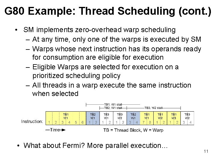
G 80 Example: Thread Scheduling (cont. ) • SM implements zero-overhead warp scheduling – At any time, only one of the warps is executed by SM – Warps whose next instruction has its operands ready for consumption are eligible for execution – Eligible Warps are selected for execution on a prioritized scheduling policy – All threads in a warp execute the same instruction when selected • What about Fermi? More parallel execution… 11

The Cache and Memory Hierarchy • Like earlier GPUs, the Fermi architecture provides for local (shared) memory in each SM • New to Fermi is the ability to use some of this local memory as a first-level (L 1) cache for global memory references. The local memory is 64 K in size, and can be split 16 K/48 K or 48 K/16 K between L 1 and shared memory • The decision to allocate 16 K or 48 K of the local memory as cache depends on two factors: how much shared memory is needed, and how predictable the kernel’s accesses to global memory. • A larger shared-memory requirement argues for less cache; more frequent or unpredictable accesses to larger regions of DRAM argues for more cache. 12

The L 2 Cache on Fermi • Each Fermi GPU is equipped with an L 2 cache (768 KB in size for a 512 -core chip). The L 2 cache covers GPU local DRAM as well as system memory • L 2 has a set of memory read-modify-write operations that are atomic for synchronization across thread blocks, or even kernels? ? – Good for mutual exclusion, but not for Barrier – implemented by a set of integer ALUs logically that can lock access to a single memory address while the read-modify-write sequence is completed – This memory address can be in system memory (cache data from CPU? ? ), in the GPU’s locally connected DRAM, or even in the memory spaces of other PCI Express connected devices – According to NVIDIA, atomic operations on Fermi are 5× to 20× faster than on previous GPUs using conventional synchronization 13

Other Features • Fermi provides six 64 -bit DRAM channels that support SDDR 3 and GDDR 5 DRAMs. Up to 6 GB of GDDR 5 DRAM can be connected to the chip • Fermi is the first GPU to provide ECC protection for DRAM; the chip’s register files, shared memories, L 1 and L 2 caches are also ECC protected. • The Giga. Thread controller that manages application context switching also provides a pair of streaming datatransfer engines, each of which can fully saturate Fermi’s PCI Express host interface. Typically, one will be used to move data from system memory to GPU memory when setting up a GPU computation, while the other will be used to move result data from GPU memory to system memory

GPU Road Map - Nvidia • Nvidia roadmap sketch: Jen-Hsun Huang (CEO of Nvidia) projects performance using an unusual, GPU-computingfocused metric: double-precision giga. FLOPS per watt, indicates power-efficiency rather than raw, peak performance. • Kepler: The next major GPU architecture from Nvidia, for release in 2011 using 28 -nanometer process. Nvidia intends for three times in DP FLOPS per watt, than Fermi. Improvement goes "far beyond" what process technology advances alone can achieve. Changes in the chip architecture, design, and software will contribute to that advance, as well. • The Maxwell architecture will come in 2013, with 22 -nm fabrication process. Maxwell promises nearly an 8 X increase in DP FLOPS per watt beyond Fermi chips. Huang noted that, in parallel computing, power is the primary constraint, which is why he chose that metric to describe future architectures. 15

Dave Patterson’s Comment on Fermi This is a preview on the Top 10 most important innovations in the new Fermi architecture as well as 3 challenges on how to bring future GPUs even closer to mainstream computing Top 10 Innovations in Fermi: 1 Real Floating Point in Quality and Performance 2 Error Correcting Codes on Main Memory and Caches 3 64‐bit Virtual Address Space 4 Caches 5 Fast Context Switching 6 Unified Address Space 7 Debugging Support 8 Faster Atomic Instructions to Support Task‐Based Parallel Programming 9 A Brand New Instruction Set 10 Also, Fermi is Faster than G 80 Top 3 Next Challenges: 1 The Relatively Small Size of GPU Memory 2 Inability to do I/O directly to GPU Memory 3 No Glueless Multisocket Hardware and Software 16

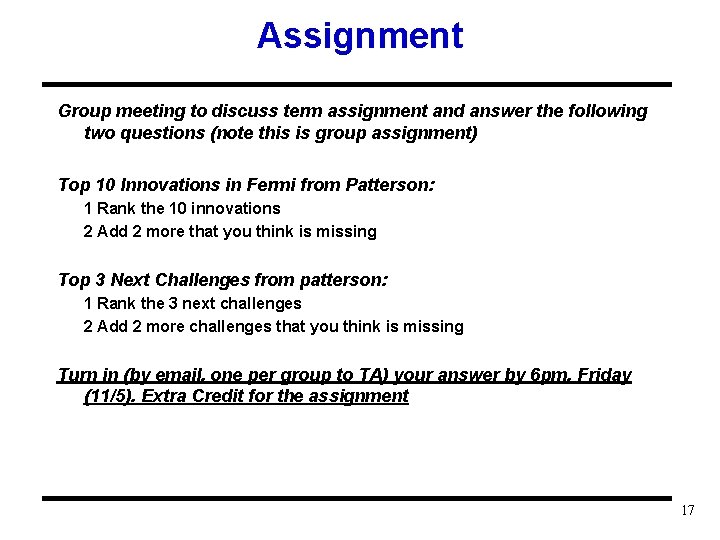
Assignment Group meeting to discuss term assignment and answer the following two questions (note this is group assignment) Top 10 Innovations in Fermi from Patterson: 1 Rank the 10 innovations 2 Add 2 more that you think is missing Top 3 Next Challenges from patterson: 1 Rank the 3 next challenges 2 Add 2 more challenges that you think is missing Turn in (by email, one per group to TA) your answer by 6 pm, Friday (11/5). Extra Credit for the assignment 17