Arria 10 HPS External Memory Interface Guidelines Quartus

- Slides: 13

Arria 10 HPS External Memory Interface Guidelines Quartus Prime Software v 17. 0

Introduction § This slide deck covers the following topics: – HPS EMIF limitations/restrictions – HPS EMIF IP generation – HPS EMIF pin constraints *EMIF = External Memory Interface 2

Software Requirements § Quartus Prime Software v 17. 0 3

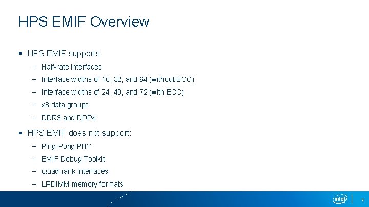
HPS EMIF Overview § HPS EMIF supports: – Half-rate interfaces – Interface widths of 16, 32, and 64 (without ECC) – Interface widths of 24, 40, and 72 (with ECC) – x 8 data groups – DDR 3 and DDR 4 § HPS EMIF does not support: – Ping-Pong PHY – EMIF Debug Toolkit – Quad-rank interfaces – LRDIMM memory formats 4

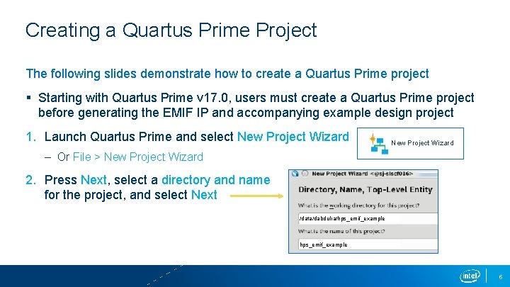
Creating a Quartus Prime Project The following slides demonstrate how to create a Quartus Prime project § Starting with Quartus Prime v 17. 0, users must create a Quartus Prime project before generating the EMIF IP and accompanying example design project 1. Launch Quartus Prime and select New Project Wizard – Or File > New Project Wizard 2. Press Next, select a directory and name for the project, and select Next /data/dabdulra/hps_emif_example 5

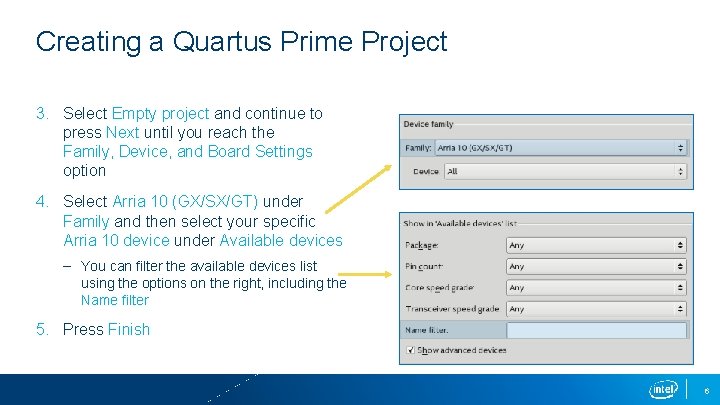
Creating a Quartus Prime Project 3. Select Empty project and continue to press Next until you reach the Family, Device, and Board Settings option 4. Select Arria 10 (GX/SX/GT) under Family and then select your specific Arria 10 device under Available devices – You can filter the available devices list using the options on the right, including the Name filter 5. Press Finish 6

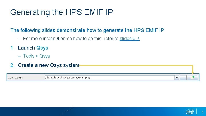
Generating the HPS EMIF IP The following slides demonstrate how to generate the HPS EMIF IP – For more information on how to do this, refer to slides 6 -7 1. Launch Qsys: – Tools > Qsys 2. Create a new Qsys system 7

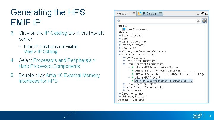
Generating the HPS EMIF IP 3. Click on the IP Catalog tab in the top-left corner – If the IP Catalog is not visible: View > IP Catalog 4. Select Processors and Peripherals > Hard Processor Components 5. Double-click Arria 10 External Memory Interfaces for HPS 8

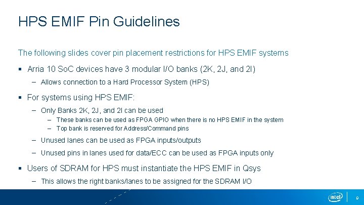
HPS EMIF Pin Guidelines The following slides cover pin placement restrictions for HPS EMIF systems § Arria 10 So. C devices have 3 modular I/O banks (2 K, 2 J, and 2 I) – Allows connection to a Hard Processor System (HPS) § For systems using HPS EMIF: – Only Banks 2 K, 2 J, and 2 I can be used – These banks can be used as FPGA GPIO when there is no HPS EMIF in the system – Top bank is reserved for Address/Command pins – Unused lanes can be used as FPGA inputs/outputs – Unused pins in lanes used for data/ECC can be used as FPGA inputs only § Users of SDRAM for HPS must instantiate the HPS EMIF in Qsys – This allows the right banks/lanes to be assigned for the SDRAM I/O 9

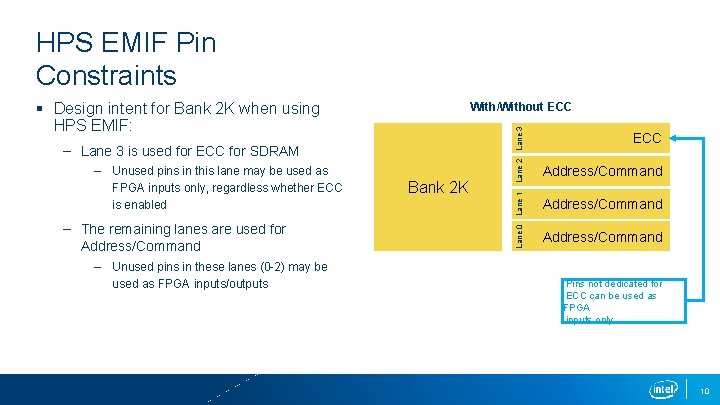
HPS EMIF Pin Constraints § Design intent for Bank 2 K when using HPS EMIF: – Unused pins in these lanes (0 -2) may be used as FPGA inputs/outputs Lane 3 – The remaining lanes are used for Address/Command Bank 2 K Lane 2 – Unused pins in this lane may be used as FPGA inputs only, regardless whether ECC is enabled ECC Address/Command Lane 1 – Lane 3 is used for ECC for SDRAM Address/Command Lane 0 With/Without ECC Address/Command Pins not dedicated for ECC can be used as FPGA inputs only 10

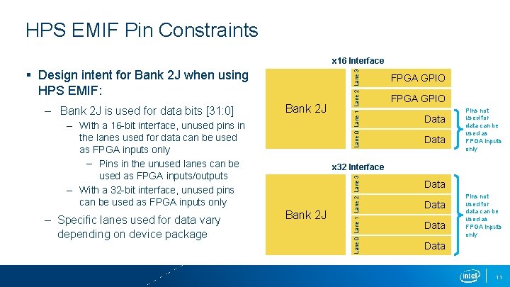
HPS EMIF Pin Constraints § Design intent for Bank 2 J when using HPS EMIF: – With a 16 -bit interface, unused pins in the lanes used for data can be used as FPGA inputs only – Pins in the unused lanes can be used as FPGA inputs/outputs – With a 32 -bit interface, unused pins can be used as FPGA inputs only – Specific lanes used for data vary depending on device package FPGA GPIO Data Pins not used for data can be used as FPGA inputs only x 32 Interface Bank 2 J Lane 0 Lane 1 Lane 2 Lane 3 – Bank 2 J is used for data bits [31: 0] Bank 2 J Lane 0 Lane 1 Lane 2 Lane 3 x 16 Interface Data Pins not used for data can be used as FPGA inputs only Data 11

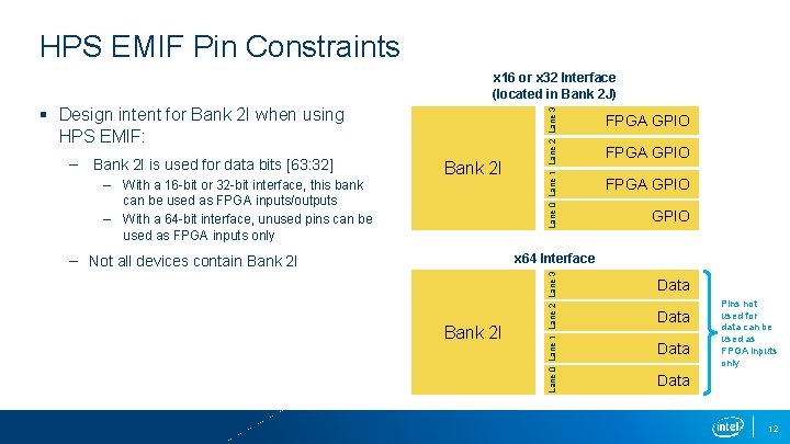
HPS EMIF Pin Constraints § Design intent for Bank 2 I when using HPS EMIF: – With a 16 -bit or 32 -bit interface, this bank can be used as FPGA inputs/outputs – With a 64 -bit interface, unused pins can be used as FPGA inputs only Bank 2 I – Not all devices contain Bank 2 I FPGA GPIO x 64 Interface Bank 2 I Lane 0 Lane 1 Lane 2 Lane 3 – Bank 2 I is used for data bits [63: 32] Lane 0 Lane 1 Lane 2 Lane 3 x 16 or x 32 Interface (located in Bank 2 J) Data Pins not used for data can be used as FPGA inputs only Data 12
