Stratix 10 External Memory Interface Pin Guidelines Quartus

- Slides: 29

Stratix 10 External Memory Interface Pin Guidelines Quartus Prime Software v 17. 0 ir 3 Stratix 10 EMIF Pin Guidelines are preliminary and subject to change

Introduction § Intel’s EMIF IP has many restrictions when it comes to pin placement § This slide deck covers the following topics: – I/O bank structure – Adjacent/Contiguous banks – Resource sharing – Pin constraints – EMIF placement § For more information regarding EMIF pin placement, refer to the Planning Pin and FPGA Resources section in the External Memory Interface Handbook *EMIF = External Memory Interface 2

Software Requirements § Quartus Prime Software v 17. 0 ir 3 3

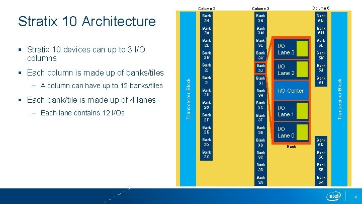
§ Stratix 10 devices can up to 3 I/O columns – A column can have up to 12 banks/tiles § Each bank/tile is made up of 4 lanes – Each lane contains 12 I/Os Transceiver Block § Each column is made up of banks/tiles Column 3 Column 5 Bank 2 N Bank 3 N Bank 5 N Bank 2 M Bank 3 M Bank 5 M Bank 2 L Bank 3 L Bank 2 K Bank 3 K Bank 2 J Bank 3 J Bank 2 I Bank 3 I Bank 2 H Bank 3 H Bank 2 G Bank 3 G Bank 2 F Bank 3 F Bank 2 E Bank 3 E Bank 2 D Bank 3 D Bank 2 C Bank 3 C Bank 5 C Bank 3 B Bank 5 B Bank 3 A Bank 5 A I/O Lane 3 I/O Lane 2 Bank 5 L Bank 5 K Bank 5 J Bank 5 I I/O Center I/O Lane 1 I/O Lane 0 Bank Transceiver Block Stratix 10 Architecture Column 2 Bank 5 D 4

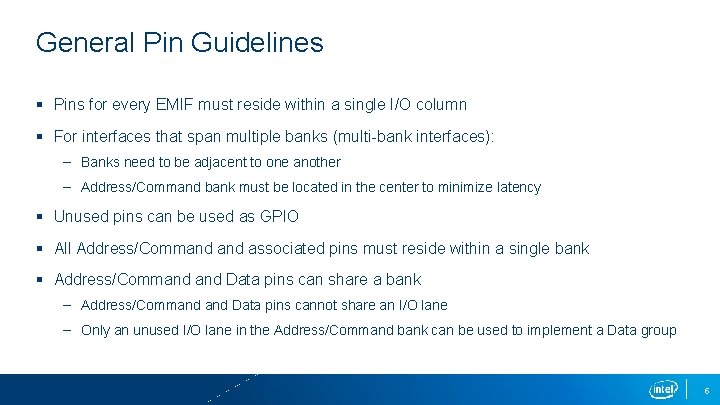
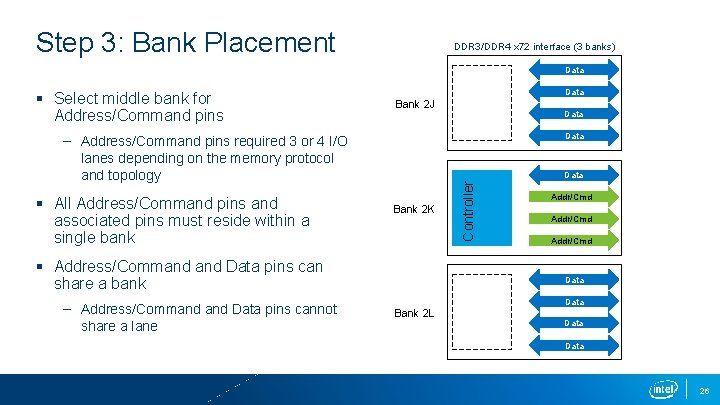
General Pin Guidelines § Pins for every EMIF must reside within a single I/O column § For interfaces that span multiple banks (multi-bank interfaces): – Banks need to be adjacent to one another – Address/Command bank must be located in the center to minimize latency § Unused pins can be used as GPIO § All Address/Command associated pins must reside within a single bank § Address/Command Data pins can share a bank – Address/Command Data pins cannot share an I/O lane – Only an unused I/O lane in the Address/Command bank can be used to implement a Data group 5

Adjacent/Contiguous Banks The following slides cover how to determine if banks are considered adjacent/contiguous § To determine if banks are adjacent/contiguous: – Refer to the Modular I/O Banks Location and Pin Counts in Stratix 10 Devices section in the Stratix 10 General Purpose I/O User Guide: § Banks need to be in the same I/O column to be considered adjacent/contiguous 6

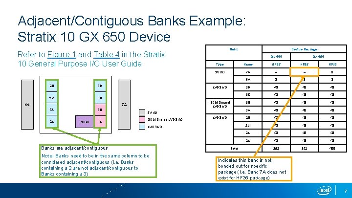
Adjacent/Contiguous Banks Example: Stratix 10 GX 650 Device Refer to Figure 1 and Table 4 in the Stratix 10 General Purpose I/O User Guide 2 N 3 D 2 M 3 C 6 A 2 K 3 B SDM 3 A Name HF 35 NF 43 3 V I/O 7 A ‒ ‒ 8 6 A 8 8 8 3 D 48 48 48 3 C 48 48 48 SDM Shared LVDS I/O 3 B 48 48 48 3 A 48 48 48 LVDS I/O 2 N 48 48 48 2 M 48 48 48 2 L 48 48 48 2 K 48 48 48 392 400 LVDS I/O Banks are adjacent/contiguous Note: Banks need to be in the same column to be considered adjacent/contiguous (i. e. Banks containing a 2 are not adjacent/contiguous to Banks containing a 3) GX 650 Type 3 V I/O SDM Shared LVDS I/O Device Package GX 400 LVDS I/O 7 A 2 L Bank Total Indicates this bank is not bonded out for specific package (i. e. Bank 7 A does not exist for HF 35 package) 7

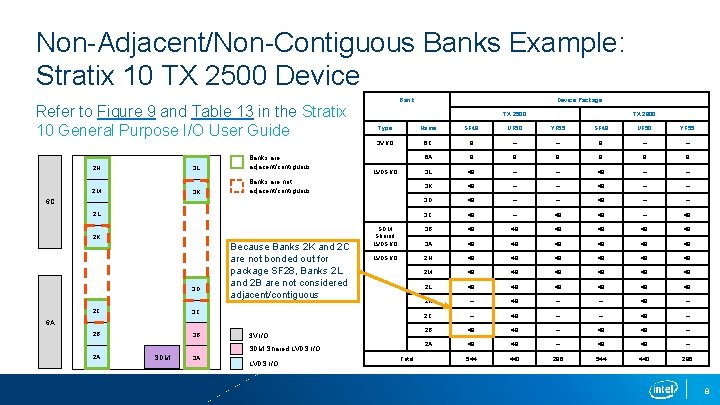
Non-Adjacent/Non-Contiguous Banks Example: Stratix 10 TX 2500 Device Refer to Figure 9 and Table 13 in the Stratix 10 General Purpose I/O User Guide 2 N 2 M 3 L Banks are adjacent/contiguous 3 K Banks are not adjacent/contiguous Bank Name SF 48 UF 50 YF 55 3 V I/O 6 C 8 ‒ ‒ 6 A 8 8 8 LVDS I/O 2 L 3 D 2 C Because Banks 2 K and 2 C are not bonded out for package SF 28, Banks 2 L and 2 B are not considered adjacent/contiguous SDM 3 A ‒ 48 ‒ ‒ 3 D 48 ‒ ‒ 48 48 48 48 3 A 48 48 48 LVDS I/O 2 N 48 48 48 2 M 48 48 48 2 L 48 48 48 2 K ‒ 48 ‒ 2 C ‒ 48 ‒ 2 B 48 48 ‒ 2 A 48 48 ‒ 544 440 296 3 V I/O LVDS I/O ‒ 48 3 B SDM Shared LVDS I/O 2 A 48 3 C 6 A 3 B 3 L 3 K SDM Shared LVDS I/O 3 C 2 B TX 2800 Type 6 C 2 K Device Package TX 2500 Total 8

I/O Bank Sharing The following slides cover requirements for sharing I/O banks § Memory interfaces can share a bank if they share the same: – Protocol – Clock (rate, frequency, PLL reference clock) – Voltage (VCCIO, VREF) § Memory interfaces cannot share: – Any given lane in a bank – Only one clock tree per lane – Address/Command bank – Interfaces cannot share the same controller or sequencer § Unused pins can be used as GPIO 9

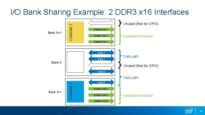
Bank N+1 Controller 1 I/O Bank Sharing Example: 2 DDR 3 x 16 Interfaces Data Unused (free for GPIO) Addr/Cmd 1 Address/Command Addr/Cmd 1 Data 1 Bank N Data path Unused (free for GPIO) Data 2 Bank N-1 Controller 2 Data path Data 2 Addr/Cmd 2 Address/Command Addr/Cmd 2 10

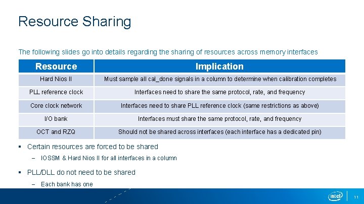
Resource Sharing The following slides go into details regarding the sharing of resources across memory interfaces Resource Implication Hard Nios II Must sample all cal_done signals in a column to determine when calibration completes PLL reference clock Interfaces need to share the same protocol, rate, and frequency Core clock network Interfaces need to share PLL reference clock (same restrictions as above) I/O bank Interfaces must share the same protocol, rate, and frequency OCT and RZQ Should not be shared across interfaces (each interface has a dedicated pin) § Certain resources are forced to be shared – IOSSM & Hard Nios II for all interfaces in a column § PLL/DLL do not need to be shared – Each bank has one 11

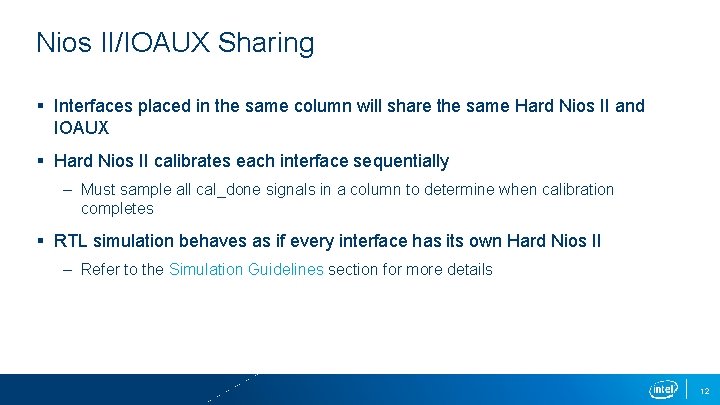
Nios II/IOAUX Sharing § Interfaces placed in the same column will share the same Hard Nios II and IOAUX § Hard Nios II calibrates each interface sequentially – Must sample all cal_done signals in a column to determine when calibration completes § RTL simulation behaves as if every interface has its own Hard Nios II – Refer to the Simulation Guidelines section for more details 12

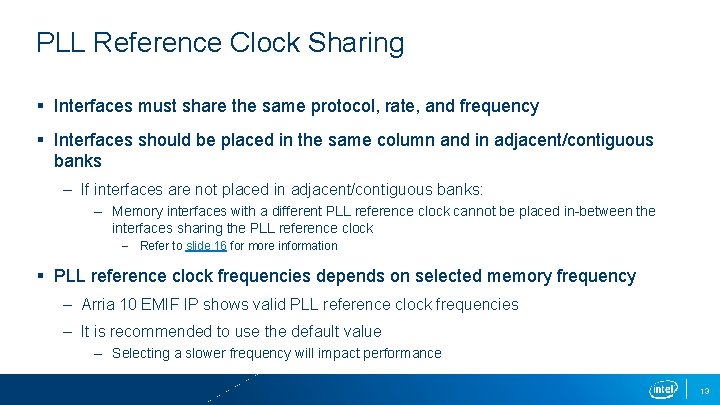
PLL Reference Clock Sharing § Interfaces must share the same protocol, rate, and frequency § Interfaces should be placed in the same column and in adjacent/contiguous banks – If interfaces are not placed in adjacent/contiguous banks: – Memory interfaces with a different PLL reference clock cannot be placed in-between the interfaces sharing the PLL reference clock – Refer to slide 16 for more information § PLL reference clock frequencies depends on selected memory frequency – Arria 10 EMIF IP shows valid PLL reference clock frequencies – It is recommended to use the default value – Selecting a slower frequency will impact performance 13

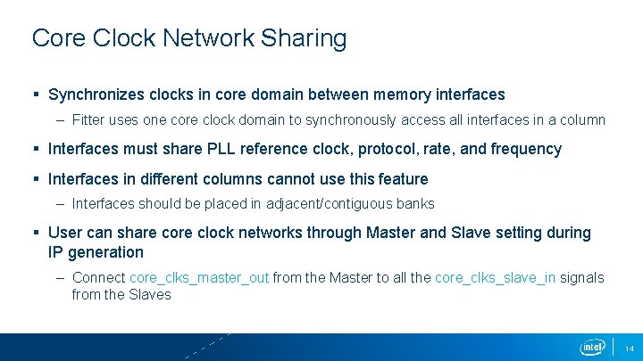
Core Clock Network Sharing § Synchronizes clocks in core domain between memory interfaces – Fitter uses one core clock domain to synchronously access all interfaces in a column § Interfaces must share PLL reference clock, protocol, rate, and frequency § Interfaces in different columns cannot use this feature – Interfaces should be placed in adjacent/contiguous banks § User can share core clock networks through Master and Slave setting during IP generation – Connect core_clks_master_out from the Master to all the core_clks_slave_in signals from the Slaves 14

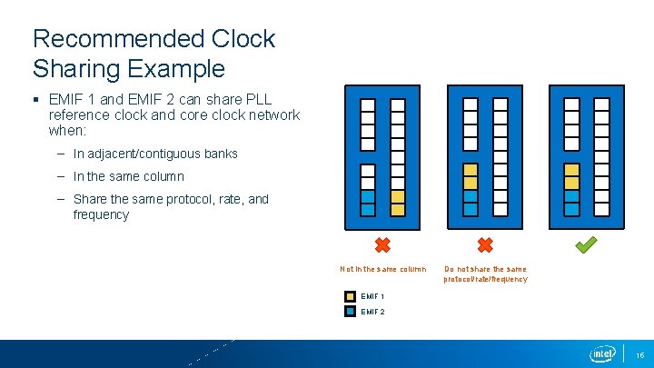
Recommended Clock Sharing Example § EMIF 1 and EMIF 2 can share PLL reference clock and core clock network when: – In adjacent/contiguous banks – In the same column – Share the same protocol, rate, and frequency Not in the same column Do not share the same protocol/rate/frequency EMIF 1 EMIF 2 15

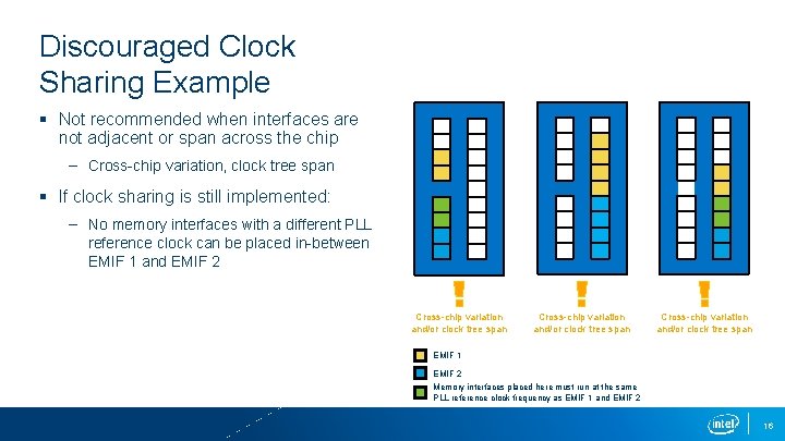
Discouraged Clock Sharing Example § Not recommended when interfaces are not adjacent or span across the chip – Cross-chip variation, clock tree span § If clock sharing is still implemented: – No memory interfaces with a different PLL reference clock can be placed in-between EMIF 1 and EMIF 2 Cross-chip variation and/or clock tree span EMIF 1 EMIF 2 Memory interfaces placed here must run at the same PLL reference clock frequency as EMIF 1 and EMIF 2 16

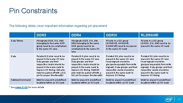
Pin Constraints The following slides cover important information regarding pin placement DDR 3 DDR 4 QDRIV RLDRAM 3 Data Strobe All signals (DQS, DQ, DM) belonging to the same DQS group need to be constrained to the same I/O lane. All signals (DQS, DQ, DM, DBI) belonging to the same DQS group need to be constrained to the same I/O lane. All pins in a DQ group (DKA/DKB, QKA/QKB, DQA/DQB) need to be placed in the same I/O bank All pins in a DQ group (DK/QK, DQ, DM) need to be placed in the same I/O bank Data Related DQ pins need to be placed in the same I/O lane. Data groups and their respective clocks should be placed in the same bank to improve I/O timing. DM pins must be paired off with a DQ pin for proper functionality 1 Related DQ pins need to be placed in the same I/O lane. Data groups and their respective clocks should be placed in the same bank to improve I/O timing. DM/DBI pins must be paired off with a DQ pin for proper functionality 1 Related DQ pins need to be placed in the same I/O lane (read signals should be grouped separately from write signals). Data groups and their respective clocks should be placed in the same bank to improve I/O timing Address/Command Must be placed in predefined locations within an I/O bank 1 See slides 21 -22 for more details 17

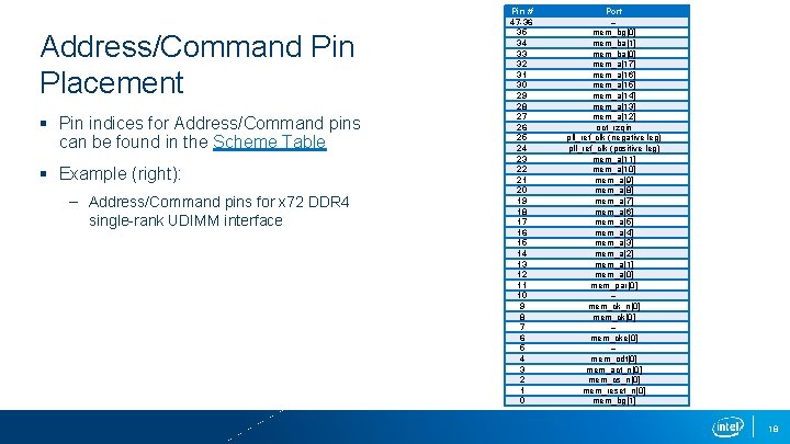
Address/Command Pin Placement § Pin indices for Address/Command pins can be found in the Scheme Table § Example (right): – Address/Command pins for x 72 DDR 4 single-rank UDIMM interface Pin # 47 -36 35 34 33 32 31 30 29 28 27 26 25 24 23 22 21 20 19 18 17 16 15 14 13 12 11 10 9 8 7 6 5 4 3 2 1 0 Port ‒ mem_bg[0] mem_ba[1] mem_ba[0] mem_a[17] mem_a[16] mem_a[15] mem_a[14] mem_a[13] mem_a[12] oct_rzqin pll_ref_clk (negative leg) pll_ref_clk (positive leg) mem_a[11] mem_a[10] mem_a[9] mem_a[8] mem_a[7] mem_a[6] mem_a[5] mem_a[4] mem_a[3] mem_a[2] mem_a[1] mem_a[0] mem_par[0] ‒ mem_ck_n[0] mem_ck[0] ‒ mem_cke[0] ‒ mem_odt[0] mem_act_n[0] mem_cs_n[0] mem_reset_n[0] mem_bg[1] 18

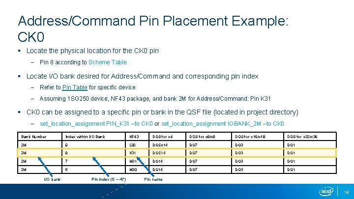
Address/Command Pin Placement Example: CK 0 § Locate the physical location for the CK 0 pin – Pin 8 according to Scheme Table § Locate I/O bank desired for Address/Command corresponding pin index – Refer to Pin Table for specific device – Assuming 1 SG 250 device, NF 43 package, and bank 2 M for Address/Command: Pin K 31 § CK 0 can be assigned to a specific pin or bank in the QSF file (located in project directory) – set_location_assignment PIN_K 31 –to CK 0 or set_location_assignment IOBANK_2 M –to CK 0 Bank Number Index within I/O Bank NF 43 DQS for x 4 DQS for x 8/x 9 DQS for x 16/x 18 DQS for x 32/x 36 2 M 9 L 30 DQSn 14 DQ 7 DQ 3 DQ 1 2 M 8 K 31 DQS 14 DQ 7 DQ 3 DQ 1 2 M 7 M 31 DQ 14 DQ 7 DQ 3 DQ 1 2 M 6 M 30 DQ 14 DQ 7 DQ 3 DQ 1 I/O bank Pin index (0 – 47) Pin name 19

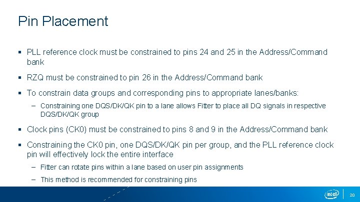
Pin Placement § PLL reference clock must be constrained to pins 24 and 25 in the Address/Command bank § RZQ must be constrained to pin 26 in the Address/Command bank § To constrain data groups and corresponding pins to appropriate lanes/banks: – Constraining one DQS/DK/QK pin to a lane allows Fitter to place all DQ signals in respective DQS/DK/QK group § Clock pins (CK 0) must be constrained to pins 8 and 9 in the Address/Command bank § Constraining the CK 0 pin, one DQS/DK/QK pin per group, and the PLL reference clock pin will effectively lock the entire interface – Fitter can rotate pins within a lane based on user pin assignments – This method is recommended for constraining pins 20

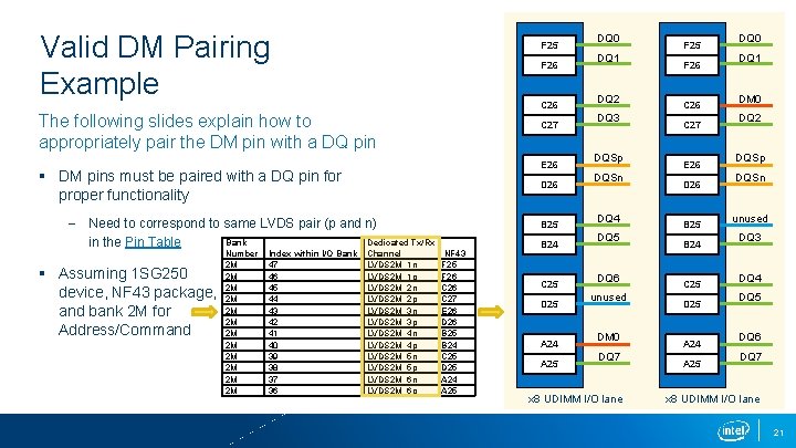
Valid DM Pairing Example F 25 F 26 C 26 The following slides explain how to appropriately pair the DM pin with a DQ pin C 27 E 26 § DM pins must be paired with a DQ pin for proper functionality D 26 – Need to correspond to same LVDS pair (p and n) Bank Dedicated Tx/Rx in the Pin Table § Assuming 1 SG 250 device, NF 43 package, and bank 2 M for Address/Command Number 2 M 2 M 2 M Index within I/O Bank 47 46 45 44 43 42 41 40 39 38 37 36 Channel LVDS 2 M_1 n LVDS 2 M_1 p LVDS 2 M_2 n LVDS 2 M_2 p LVDS 2 M_3 n LVDS 2 M_3 p LVDS 2 M_4 n LVDS 2 M_4 p LVDS 2 M_5 n LVDS 2 M_5 p LVDS 2 M_6 n LVDS 2 M_6 p B 25 NF 43 F 25 F 26 C 27 E 26 D 26 B 25 B 24 C 25 D 25 A 24 A 25 DQ 0 DQ 1 DQ 2 DQ 3 DQSp DQSn DQ 4 DQ 5 DQ 6 unused DM 0 DQ 7 x 8 UDIMM I/O lane F 25 F 26 C 27 E 26 D 26 B 25 B 24 C 25 D 25 A 24 A 25 DQ 0 DQ 1 DM 0 DQ 2 DQSp DQSn unused DQ 3 DQ 4 DQ 5 DQ 6 DQ 7 x 8 UDIMM I/O lane 21

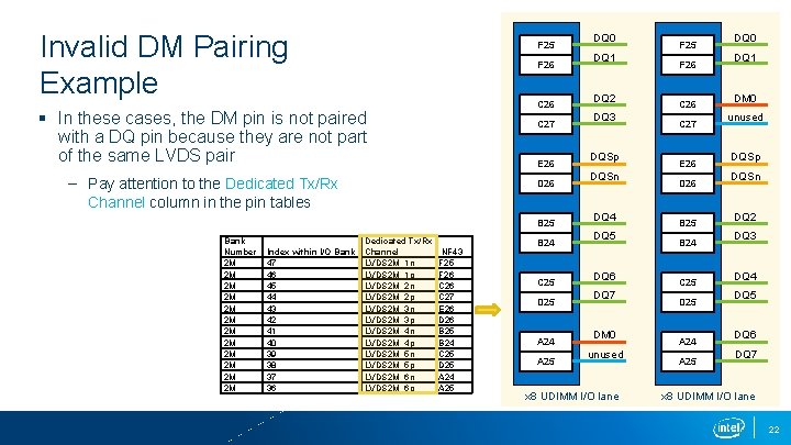
Invalid DM Pairing Example F 25 F 26 C 26 § In these cases, the DM pin is not paired with a DQ pin because they are not part of the same LVDS pair C 27 E 26 – Pay attention to the Dedicated Tx/Rx Channel column in the pin tables D 26 B 25 Bank Number 2 M 2 M 2 M Index within I/O Bank 47 46 45 44 43 42 41 40 39 38 37 36 Dedicated Tx/Rx Channel LVDS 2 M_1 n LVDS 2 M_1 p LVDS 2 M_2 n LVDS 2 M_2 p LVDS 2 M_3 n LVDS 2 M_3 p LVDS 2 M_4 n LVDS 2 M_4 p LVDS 2 M_5 n LVDS 2 M_5 p LVDS 2 M_6 n LVDS 2 M_6 p NF 43 F 25 F 26 C 27 E 26 D 26 B 25 B 24 C 25 D 25 A 24 A 25 DQ 0 DQ 1 DQ 2 DQ 3 DQSp DQSn DQ 4 DQ 5 DQ 6 DQ 7 DM 0 unused x 8 UDIMM I/O lane F 25 F 26 C 27 E 26 D 26 B 25 B 24 C 25 D 25 A 24 A 25 DQ 0 DQ 1 DM 0 unused DQSp DQSn DQ 2 DQ 3 DQ 4 DQ 5 DQ 6 DQ 7 x 8 UDIMM I/O lane 22

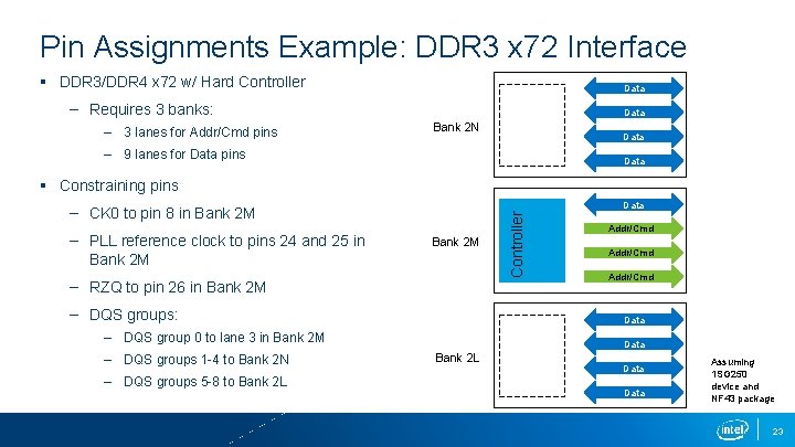
Pin Assignments Example: DDR 3 x 72 Interface § DDR 3/DDR 4 x 72 w/ Hard Controller Data – Requires 3 banks: – 3 lanes for Addr/Cmd pins Data Bank 2 N Data – 9 lanes for Data pins Data § Constraining pins – PLL reference clock to pins 24 and 25 in Bank 2 M – RZQ to pin 26 in Bank 2 M – DQS groups: – DQS groups 5 -8 to Bank 2 L Addr/Cmd Data – DQS group 0 to lane 3 in Bank 2 M – DQS groups 1 -4 to Bank 2 N Controller Data – CK 0 to pin 8 in Bank 2 M Data Bank 2 L Data Assuming 1 SG 250 device and NF 43 package 23

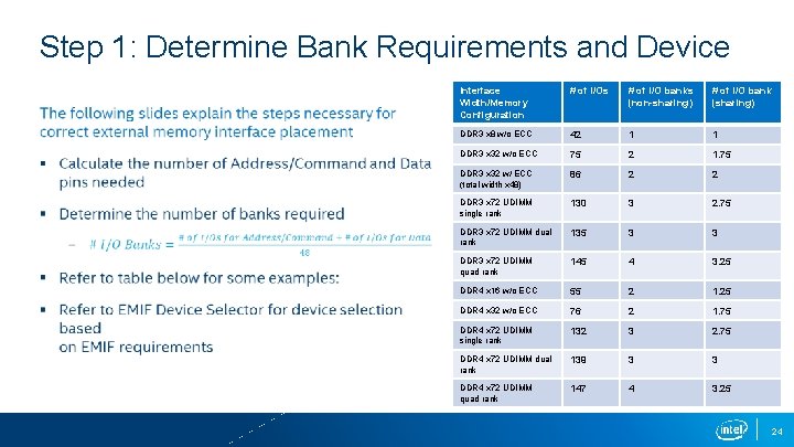
Step 1: Determine Bank Requirements and Device Interface Width/Memory Configuration # of I/Os # of I/O banks (non-sharing) # of I/O bank (sharing) DDR 3 x 8 w/o ECC 42 1 1 DDR 3 x 32 w/o ECC 75 2 1. 75 DDR 3 x 32 w/ ECC (total width x 48) 86 2 2 DDR 3 x 72 UDIMM single rank 130 3 2. 75 DDR 3 x 72 UDIMM dual rank 135 3 3 DDR 3 x 72 UDIMM quad rank 145 4 3. 25 DDR 4 x 16 w/o ECC 55 2 1. 25 DDR 4 x 32 w/o ECC 76 2 1. 75 DDR 4 x 72 UDIMM single rank 132 3 2. 75 DDR 4 x 72 UDIMM dual rank 139 3 3 DDR 4 x 72 UDIMM quad rank 147 4 3. 25 24

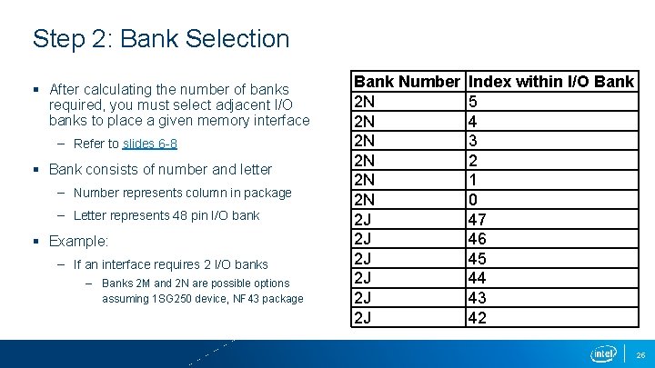
Step 2: Bank Selection § After calculating the number of banks required, you must select adjacent I/O banks to place a given memory interface – Refer to slides 6 -8 § Bank consists of number and letter – Number represents column in package – Letter represents 48 pin I/O bank § Example: – If an interface requires 2 I/O banks – Banks 2 M and 2 N are possible options assuming 1 SG 250 device, NF 43 package Bank Number 2 N 2 N 2 N 2 J 2 J 2 J Index within I/O Bank 5 4 3 2 1 0 47 46 45 44 43 42 25

Step 3: Bank Placement DDR 3/DDR 4 x 72 interface (3 banks) Data Bank 2 J – Address/Command pins required 3 or 4 I/O lanes depending on the memory protocol and topology § All Address/Command pins and associated pins must reside within a single bank Data Bank 2 K § Address/Command Data pins can share a bank – Address/Command Data pins cannot share a lane Data Controller § Select middle bank for Address/Command pins Addr/Cmd Data Bank 2 L Data 26

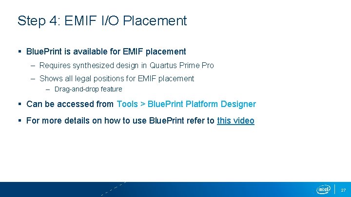
Step 4: EMIF I/O Placement § Blue. Print is available for EMIF placement – Requires synthesized design in Quartus Prime Pro – Shows all legal positions for EMIF placement – Drag-and-drop feature § Can be accessed from Tools > Blue. Print Platform Designer § For more details on how to use Blue. Print refer to this video 27

Alternative Methods for EMIF Placement § Manually constrain all interface signals to pin locations – Plan interface placement in columns (I/O bank selection – Use pin tables to find legal positions for each interface pin – Assign pin locations in QSF – Fast periphery placement – Can be lengthy process (especially with multiple IPs) § Manually constrain some interface signals and let Fitter handle the rest – Requires constraining the CK 0 pin, one DQS/DK/QK pin per group, and the PLL reference clock pin for each memory interface – Fitter can rotate pins within a lane based on user pin assignments – This method is recommended for constraining pins 28
