Thermal Aware EM Computation Imran qureshi imran qureshicenttech

- Slides: 1

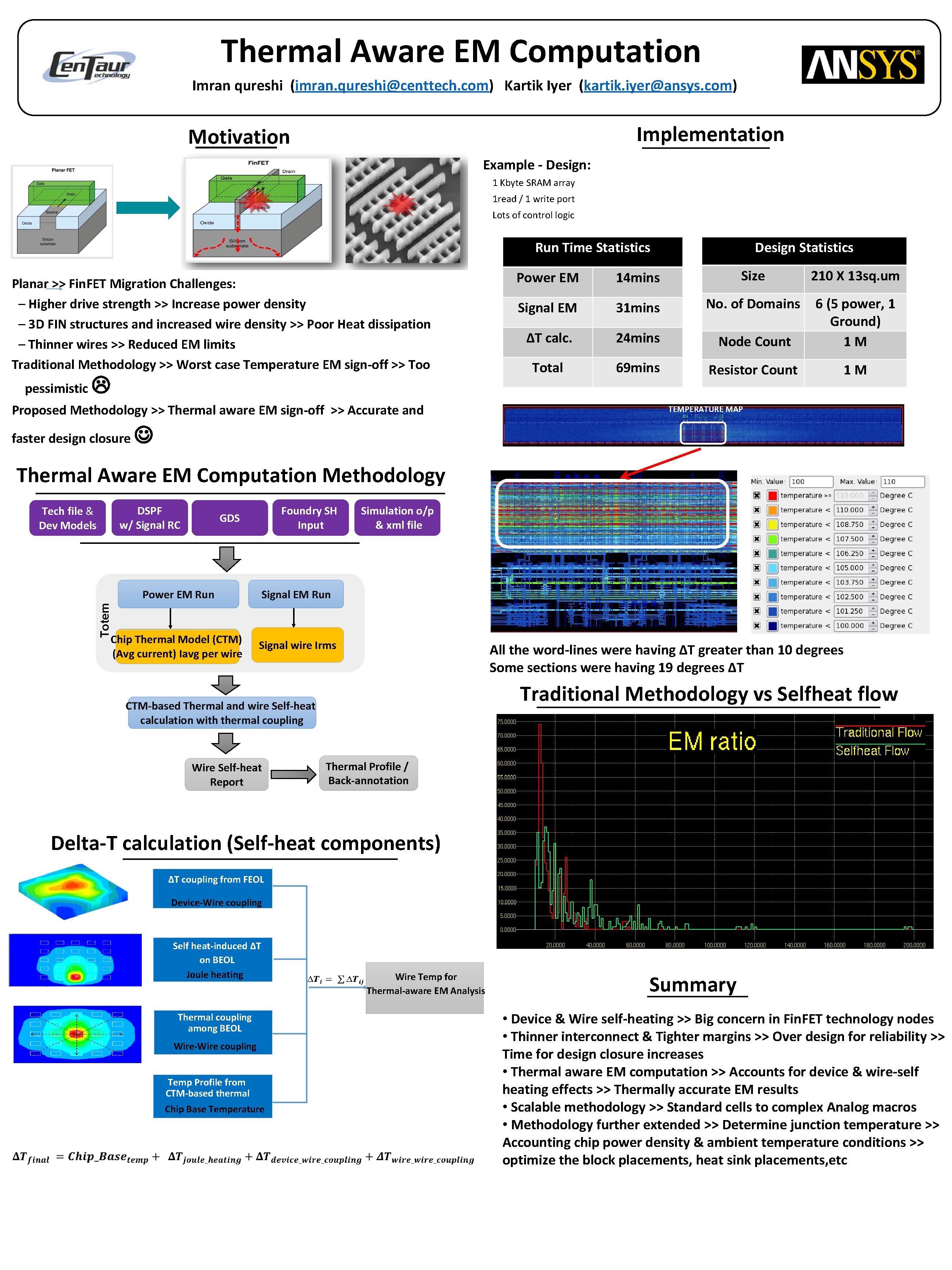
Thermal Aware EM Computation Imran qureshi (imran. qureshi@centtech. com) Kartik Iyer (kartik. iyer@ansys. com) Implementation Motivation Example - Design: 1 Kbyte SRAM array 1 read / 1 write port Lots of control logic Run Time Statistics Planar >> Fin. FET Migration Challenges: – Higher drive strength >> Increase power density – 3 D FIN structures and increased wire density >> Poor Heat dissipation – Thinner wires >> Reduced EM limits Traditional Methodology >> Worst case Temperature EM sign-off >> Too pessimistic Proposed Methodology >> Thermal aware EM sign-off >> Accurate and Design Statistics Power EM 14 mins Size 210 X 13 sq. um Signal EM 31 mins No. of Domains ∆T calc. 24 mins Node Count 6 (5 power, 1 Ground) 1 M Total 69 mins Resistor Count 1 M TEMPERATURE MAP faster design closure Thermal Aware EM Computation Methodology DSPF w/ Signal RC Tech file & Dev Models Foundry SH Input GDS Signal EM Run Chip Thermal Model (CTM) (Avg current) Iavg per wire Signal wire Irms Totem Power EM Run Simulation o/p & xml file All the word-lines were having ΔT greater than 10 degrees Some sections were having 19 degrees ΔT CTM-based Thermal and wire Self-heat calculation with thermal coupling Wire Self-heat Report Traditional Methodology vs Selfheat flow Thermal Profile / Back-annotation Delta-T calculation (Self-heat components) ∆T coupling from FEOL Device-Wire coupling Self heat-induced ∆T on BEOL Joule heating Thermal coupling among BEOL Wire-Wire coupling Temp Profile from CTM-based thermal Chip Base Temperature Wire Temp for Thermal-aware EM Analysis Summary • Device & Wire self-heating >> Big concern in Fin. FET technology nodes • Thinner interconnect & Tighter margins >> Over design for reliability >> Time for design closure increases • Thermal aware EM computation >> Accounts for device & wire-self heating effects >> Thermally accurate EM results • Scalable methodology >> Standard cells to complex Analog macros • Methodology further extended >> Determine junction temperature >> Accounting chip power density & ambient temperature conditions >> optimize the block placements, heat sink placements, etc