Synchronization of Clocked FieldCoupled Circuits Frank Sill Torres

- Slides: 1

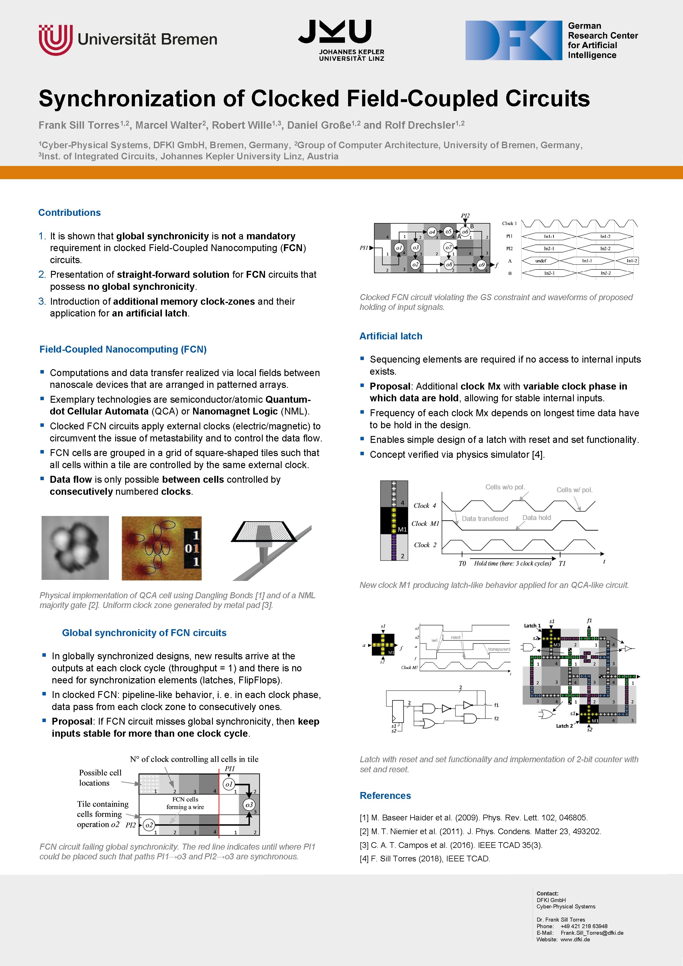
Synchronization of Clocked Field-Coupled Circuits Frank Sill Torres 1, 2, Marcel Walter 2, Robert Wille 1, 3, Daniel Große 1, 2 and Rolf Drechsler 1, 2 1 Cyber-Physical Systems, DFKI Gmb. H, Bremen, Germany, 2 Group of Computer Architecture, University of Bremen, Germany, 3 Inst. of Integrated Circuits, Johannes Kepler University Linz, Austria Contributions 1. It is shown that global synchronicity is not a mandatory requirement in clocked Field-Coupled Nanocomputing (FCN) circuits. 2. Presentation of straight-forward solution for FCN circuits that possess no global synchronicity. 3. Introduction of additional memory clock-zones and their application for an artificial latch. Clocked FCN circuit violating the GS constraint and waveforms of proposed holding of input signals. Artificial latch Field-Coupled Nanocomputing (FCN) § Computations and data transfer realized via local fields between nanoscale devices that are arranged in patterned arrays. § Exemplary technologies are semiconductor/atomic Quantumdot Cellular Automata (QCA) or Nanomagnet Logic (NML). § Clocked FCN circuits apply external clocks (electric/magnetic) to circumvent the issue of metastability and to control the data flow. § FCN cells are grouped in a grid of square-shaped tiles such that all cells within a tile are controlled by the same external clock. § Sequencing elements are required if no access to internal inputs exists. § Proposal: Additional clock Mx with variable clock phase in which data are hold, allowing for stable internal inputs. § Frequency of each clock Mx depends on longest time data have to be hold in the design. § Enables simple design of a latch with reset and set functionality. § Concept verified via physics simulator [4]. § Data flow is only possible between cells controlled by consecutively numbered clocks. New clock M 1 producing latch-like behavior applied for an QCA-like circuit. Physical implementation of QCA cell using Dangling Bonds [1] and of a NML majority gate [2]. Uniform clock zone generated by metal pad [3]. Global synchronicity of FCN circuits § In globally synchronized designs, new results arrive at the outputs at each clock cycle (throughput = 1) and there is no need for synchronization elements (latches, Flip. Flops). § In clocked FCN: pipeline-like behavior, i. e. in each clock phase, data pass from each clock zone to consecutively ones. § Proposal: If FCN circuit misses global synchronicity, then keep inputs stable for more than one clock cycle. Latch with reset and set functionality and implementation of 2 -bit counter with set and reset. References [1] M. Baseer Haider et al. (2009). Phys. Rev. Lett. 102, 046805. [2] M. T. Niemier et al. (2011). J. Phys. Condens. Matter 23, 493202. FCN circuit failing global synchronicity. The red line indicates until where PI 1 could be placed such that paths PI 1→o 3 and PI 2→o 3 are synchronous. [3] C. A. T. Campos et al. (2016). IEEE TCAD 35(3). [4] F. Sill Torres (2018), IEEE TCAD. Contact: DFKI Gmb. H Cyber-Physical Systems Dr. Frank Sill Torres Phone: +49 421 218 63948 E-Mail: Frank. Sill_Torres@dfki. de Website: www. dfki. de