Surface NanoStructuring Group Prof Dr Yong Lei yong
- Slides: 1
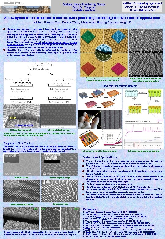
Surface Nano-Structuring Group Prof. Dr. Yong Lei yong. lei@uni-muenster. de Institut für Materialphysik and Center for Nanotechnology Universität Münster A new hybrid three-dimensional surface nano-patterning technology for nano-device applications Hui Sun, Liaoyong Wen, Kin-Mun Wong, Fabian Grote, Huaping Zhao, and Yong Lei* Surface nano-patterning has been intensively investigated for wide applications in different nano-devices. Existing surface patterning techniques have application restrictions. Realizing a surface nanopatterning with a process featured by flexibility, high throughput, low cost, and high structural controllability presents an important issue. We proposed the UTAM (ultra-thin alumina mask) surface nano-patterning technique to fabricate large-scale ordered arrays of surface nano-structures (dots, holes, wires, and tubes). Recently, the UTAM technique is advanced to realize a threedimensional surface nano-patterning technique to prepare highperformance nano-devices. Ordered quantum-sized nanodot arrays (Inside cover page of Journal ‘Small’) Highly ordered Zn. O nanotube arrays using atomic layer deposition Nano-device demonstration UTAM ordered nanodots (d 1) Nanodots (top view) (d 2) Nanoholes (top view) (b) Schematic outline of the fabrication processes of nanodot (a-b 1 -c 1 -d 1) and nanohole (a-b 2 -c 2 -d 2) arrays on Si substrates. Shape and Size Tuning The size of the UTAM-prepared nanodots can be adjusted from about 10 to 200 nm while the shapes of the nanodots can be adjusted from nanometer-sized discs, hemispheres, hemiellipsoids, to conics. Zn. O nanowire Schottky diode fabrication Zn. O nanotube gas sensing response Features and Applications Nanodisc arrays The controllability of the size, spacing, and shape allows tuning the properties of the UTAM-prepared ordered surface nanostructures. The UTAM technique is a general applicability in fabricating a wide range of ordered surface nanostructures. UTAM surface patterning can be advanced to three-dimensional surface nano-structuring. Highly ordered quantum sized nanodot arrays and free-standing onedimensional surface nanostructure arrays can be prepared using the UTAM surface nano-patterning technique. Flexible nanowire diodes were demonstrated. Nanotube based gas sensors with high sensitivity were shown. Multi-layer metallic nanodot (Fe/Pt) arrays were prepared using the UTAM technique and can be used for magenetic memory devices. UTAM-prepared nanowire/nanohole composite structure could be used to realize a high-efficient nano-generator to power implantable bio-medical devices. Nanohemisphere arrays Nanoconic arrays Nano-hemiellipsoid arrays (a) (b 1) (b 2) Three-dimensional UTAM nano-patterning to prepare free-standing 1 D surface nanostructures: Ni nanowire (a) and carbon nanotube arrays (b). References: 1. Lei Y. , et al. , Chemical Society Reviews, 40, 1247 -1258 (2011). 2. Wen L. Y. , Lei Y. , et al. , Journal of Materials Chemistry, 21, 7090 (2011) 3. Ostendorp S, Lei Y. , and Wilde G. , Chemical Physics Letters, 513, 99 (2011). 4. Wu M. H. , Wen L. Y. , Lei Y. , et al. , Small, 6, 695 -699 (2010). 5. Wen L. Y. , Lei Y. , et al. , Applied Physics Letters, 97, 053106 (2010) 6. Lei Y. , Cai W. P. , Wilde G. , Progress in Materials Science, 52, 465 -539 (2007). 7. Lei Y. , Jiao Z. , Wu M. H. , Wilde G. , Advanced Engineering Materials, 9, 343 (2007). 8. Lei Y. , Chim W. K. , Chemistry of Materials, 17, 580 (2005). 9. Lei Y. , Chim W. K. , Journal of the American Chemical Society, 127, 1487 (2005). 10. Lei Y. , Chim W. K. , Sun H. P. , Wilde G. , Applied Physics Letters, 86, 103106 (2005). 11. Lei Y. , Yeong K. S. , Thong J. T. L. , Chim W. K. , Chemistry of Materials, 16, 2757 (2004). 12. Ellrich J. , Lei Y. , Hahn H. , German Patent (2009).