SEMICONDUCTOR MATERIALS FOR SOLAR CELLS ENE 304 Materials
- Slides: 10

SEMICONDUCTOR MATERIALS FOR SOLAR CELLS ENE 304 Materials in Energy Technologies

Content • Semiconductor properties: Carrier concentrations • Semiconductor properties: Transport properties • Semiconductor properties: Recombination and generation

Semiconductor properties Carrier concentrations • In an intrinsic Si atom, electrons are allowed to have only discrete energy values, known as orbitals. • Periodic atomic structure of the single crystal silicon gives rise to the ranges of allowed energy states for electrons known as energy bands and the excluded energy ranges, band gap. • The electrons released from the bonds determine the amount of charge carried by a semiconductor. • The valence electrons in the covalent bonds have the allowed energies in the valence band (VB) and the allowed energies of the electrons released from the covalent bonds form the conduction band (CB).

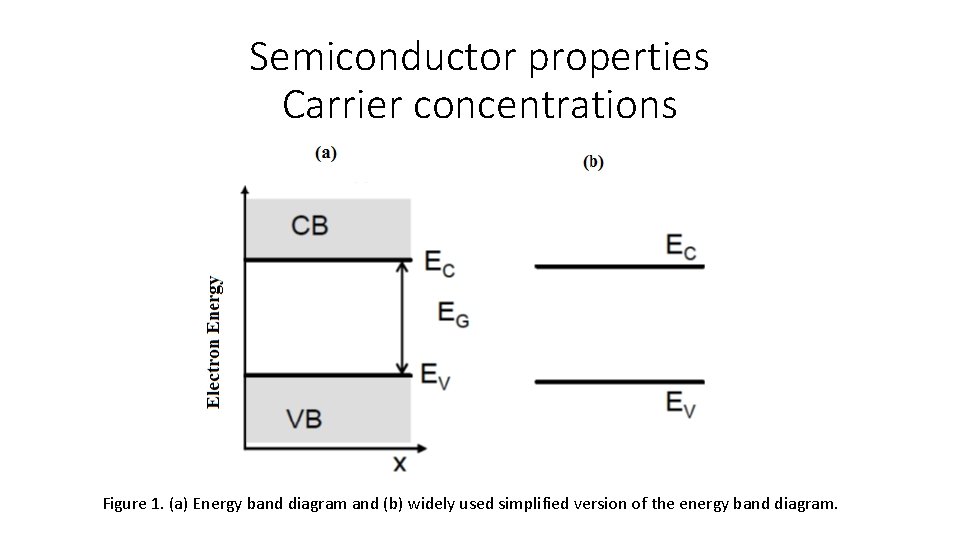
Semiconductor properties Carrier concentrations • The fobidden energy level known as band gap separates the valence band from the conduction band. • The maximum allowed energy level in the valence-band is denoted EV, and the minimum allowed energy level in the conduction-band is denoted EC. • The energy difference between Ec and Ev energy levels of these two bands is called the band gap energy or band gap, EG. • The band gap of the silicon crystal is nearly 1. 1 e. V at room temperature.

Semiconductor properties Carrier concentrations Figure 1. (a) Energy band diagram and (b) widely used simplified version of the energy band diagram.

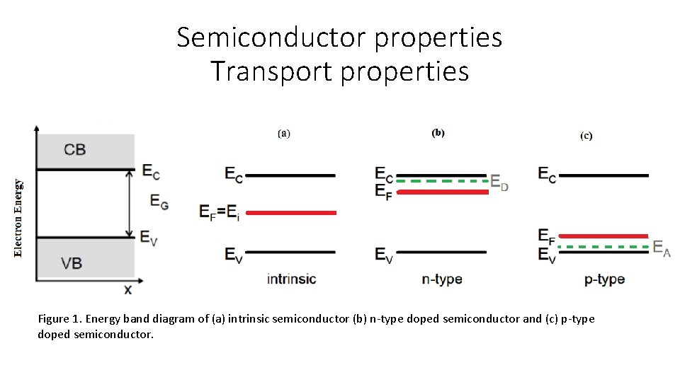
Semiconductor properties Carrier concentrations • Placing the donor and acceptor atoms in the crystal lattice of silicon brings the allowed energy levels within the forbidden band gap. • The fifth valence electron of the phosphorus atom does not play a role in forming a bond, therefore it binds weakly to the atom and easily rid of the phosphorus atom. • The energy of the released electron lies in the conducting band. • The weakly bound valence electrons of the donor atoms must be placed in an energy level, ED, close to the conducting band, which means, that an electron that occupies the ED level, is localized near the donor atom.

Semiconductor properties Transport properties Figure 1. Energy band diagram of (a) intrinsic semiconductor (b) n-type doped semiconductor and (c) p-type doped semiconductor.

Semiconductor properties Transport properties • Similarly, the acceptor atoms bring the allowed energy levels EA near the valence band. • Doping also affects the position of the Fermi energy. • While increasing the concentration of electrons by increasing concentration, the Fermi energy will also increase, making it closer to the conducting band CB as shown in Figure 2. • In P-type material, Fermi energy moves close to the valence band, which is also illustrated in Figure 2.

Semiconductor properties Recombination and generation • The electron and hole concentrations change from their equilibrium values when a semiconductor is disturbed from the equilibrium state. • In order to correct the equilibrium conditions, a series of operations begin within the semiconductor after perturbation. • Creation is a process at which electrons and holes are created. • Recombination is a process at which electrons and holes are destroyed following the generation process. • A number of semiconducting processes can occur, leading to the formation and disappearance of electrons and holes.

References • https: //ocw. tudelft. nl/wp-content/uploads/Solar-Cells-R 3 CH 3_Solar_cell_materials. pdf (04. 01. 2018) • https: //courses. edx. org/c 4 x/Delft. X/ET. 3034 TU/asset/solar_energy_v 1. 1. pdf (04. 01. 2018) • http: //alan. ece. gatech. edu/ECE 4833/Lectures/Lecture 3_Introduction 2 Semicond uctors. pdf (04. 01. 2018)