Seamless cavities via copper electrodeposition TTC 2020 CERN

- Slides: 15

Seamless cavities via copper electrodeposition TTC 2020 CERN 4 -7 February 2020 • • Lucia Lain Amador, L. Ferreira, C. Garion, E. Garcia-Tabares, T. Koettig, M. Meyer, A. T. Perez Fontenla, K. Puthran, G. Rosaz, M. Sitko and M. Taborelli This R&D program is supported by KT funding

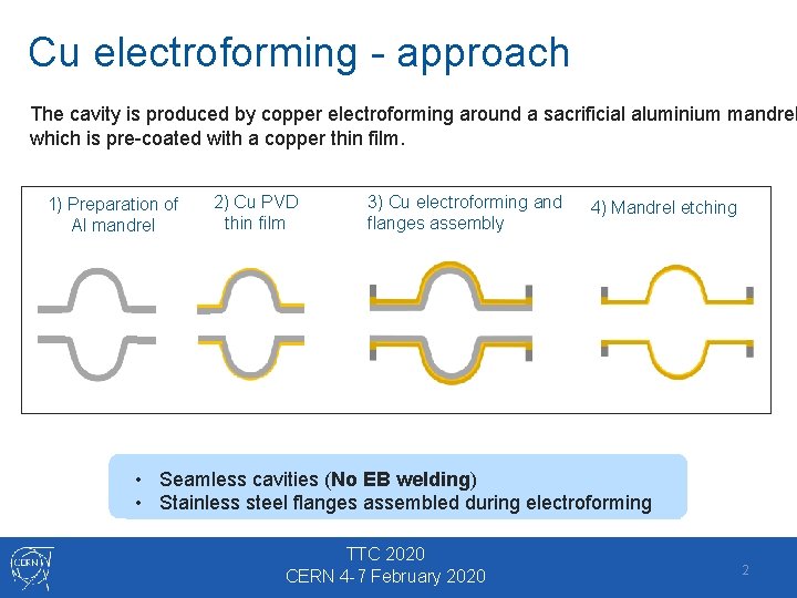
Cu electroforming - approach The cavity is produced by copper electroforming around a sacrificial aluminium mandrel which is pre-coated with a copper thin film. 1) Preparation of Al mandrel 2) Cu PVD thin film 3) Cu electroforming and flanges assembly 4) Mandrel etching • Seamless cavities (No EB welding) • Stainless steel flanges assembled during electroforming TTC 2020 CERN 4 -7 February 2020 2

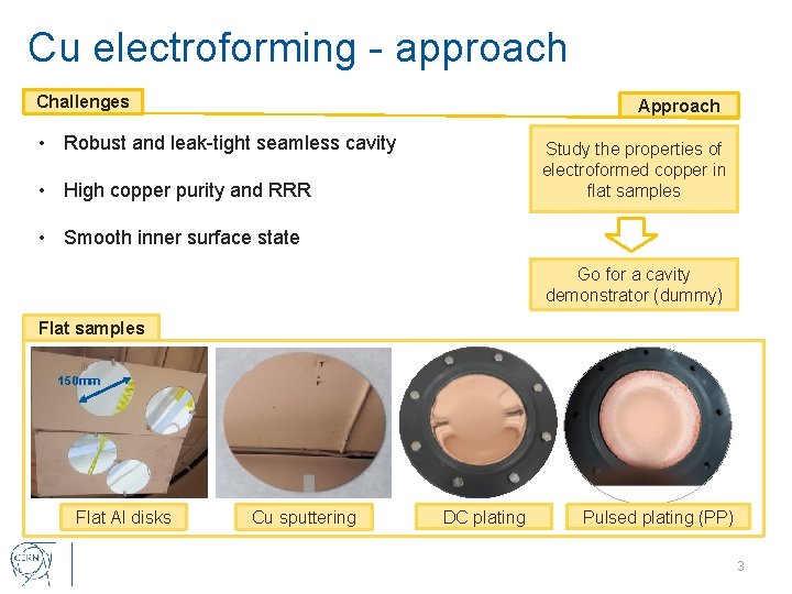
Cu electroforming - approach Challenges Approach • Robust and leak-tight seamless cavity Study the properties of electroformed copper in flat samples • High copper purity and RRR • Smooth inner surface state Go for a cavity demonstrator (dummy) Flat samples 150 mm Flat Al disks Cu sputtering DC plating Pulsed plating (PP) 3

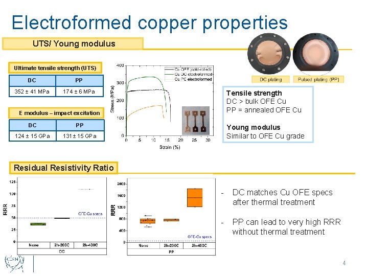
Electroformed copper properties UTS/ Young modulus Ultimate tensile strength (UTS) DC PP 352 ± 41 MPa 174 ± 6 MPa Tensile strength DC > bulk OFE Cu PP = annealed OFE Cu E modulus – impact excitation DC PP 124 ± 15 GPa 131± 15 GPa Young modulus Similar to OFE Cu grade Residual Resistivity Ratio - DC matches Cu OFE specs after thermal treatment - PP can lead to very high RRR without thermal treatment 4

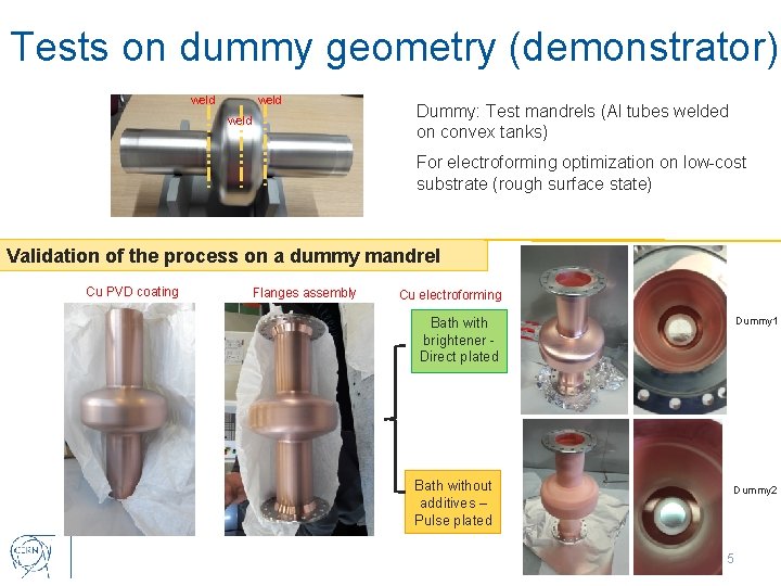
Tests on dummy geometry (demonstrator) weld Dummy: Test mandrels (Al tubes welded on convex tanks) For electroforming optimization on low-cost substrate (rough surface state) Validation of the process on a dummy mandrel Cu PVD coating Flanges assembly Cu electroforming Dummy 1 Bath with brightener Direct plated Bath without additives – Pulse plated Dummy 2 5

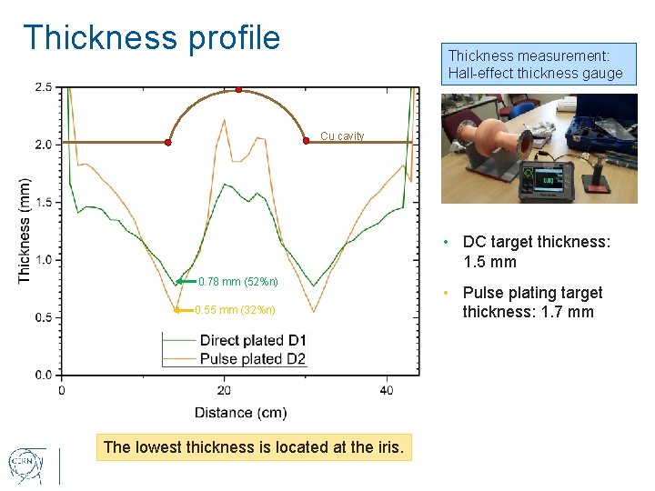
Thickness profile Thickness measurement: Hall-effect thickness gauge Cu cavity • DC target thickness: 1. 5 mm 0. 78 mm (52%n) 0. 55 mm (32%n) The lowest thickness is located at the iris. • Pulse plating target thickness: 1. 7 mm

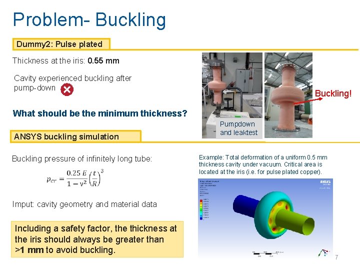
Problem- Buckling Dummy 2: Pulse plated Thickness at the iris: 0. 55 mm Cavity experienced buckling after pump-down Buckling! What should be the minimum thickness? ANSYS buckling simulation Buckling pressure of infinitely long tube: Pumpdown and leaktest Example: Total deformation of a uniform 0. 5 mm thickness cavity under vacuum. Critical area is located at the iris (i. e. for pulse plated copper). Imput: cavity geometry and material data Including a safety factor, the thickness at the iris should always be greater than >1 mm to avoid buckling. 7

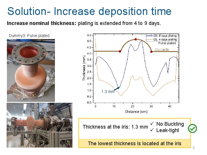
Solution- Increase deposition time Increase nominal thickness: plating is extended from 4 to 9 days. Dummy 3: Pulse plated Cu cavity 1. 3 mm Thickness at the iris: 1. 3 mm ü No Buckling ü Leak-tight The lowest thickness is located at the iris 8

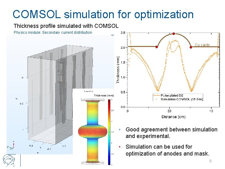
COMSOL simulation for optimization Thickness profile simulated with COMSOL Physics module: Secondary current distribution Cu cavity Thickness (mm) • Good agreement between simulation and experimental. • Simulation can be used for optimization of anodes and mask. 9

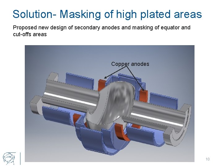
Solution- Masking of high plated areas Proposed new design of secondary anodes and masking of equator and cut-offs areas Copper anodes 10

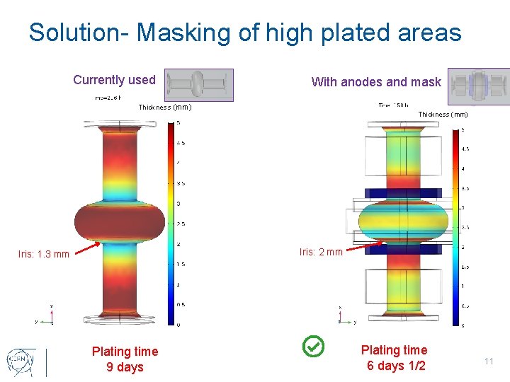
Solution- Masking of high plated areas Currently used With anodes and mask Thickness (mm) Iris: 1. 3 mm Thickening in the Plating timeequator 9 days Thickness (mm) Iris: 2 mm Thickening in the iris Plating time (critical area)1/2 6 days 11

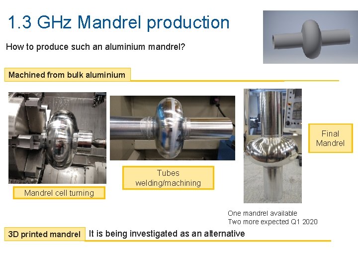
1. 3 GHz Mandrel production How to produce such an aluminium mandrel? Machined from bulk aluminium Final Mandrel Tubes welding/machining Mandrel cell turning One mandrel available Two more expected Q 1 2020 3 D printed mandrel It is being investigated as an alternative

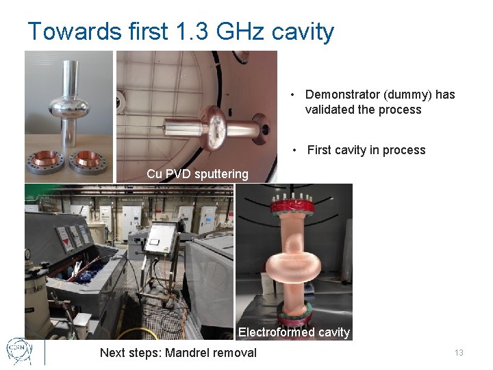
Towards first 1. 3 GHz cavity • Demonstrator (dummy) has validated the process • First cavity in process Cu PVD sputtering Electroformed cavity Next steps: Mandrel removal 13

Conclusions/perspectives • Electroformed copper has been characterized RRR up to 1600 upon thermal treatment Mechanical properties comparable to OFE-Cu or annealed OFE-Cu Roughness controlled by mandrel surface state (not shown here) • Process viability has been demonstrated with the electroformed dummies Next steps • Real 1. 3 GHz cavity in process • Study the copper surface state after etching (electroforming on polished mandrels). • Nb thin film coating using best recipe (G. Rosaz) and RF testing 14

Thank you for your attention! 15