ScanFlash ADC Low Power HighThroughput AD Converters Melvin
![Target Specifications • • 2 Channels [2 -Scan-Flash ADC] 12 bit per channel Power Target Specifications • • 2 Channels [2 -Scan-Flash ADC] 12 bit per channel Power](https://slidetodoc.com/presentation_image/2370644414ef451b7ea496f869d75355/image-9.jpg)
- Slides: 11

Scan-Flash ADC Low Power, High-Throughput AD Converters Melvin Eze Pennsylvania State University eze@cse. psu. edu Spring 2006 CSE 597 A: Analog-Digital IC Design

Outline • • • ADC Converters Flash ADC Scan-Flash Architecture Target Specifications Schedule References Spring 2006 CSE 597 A: Analog-Digital IC Design

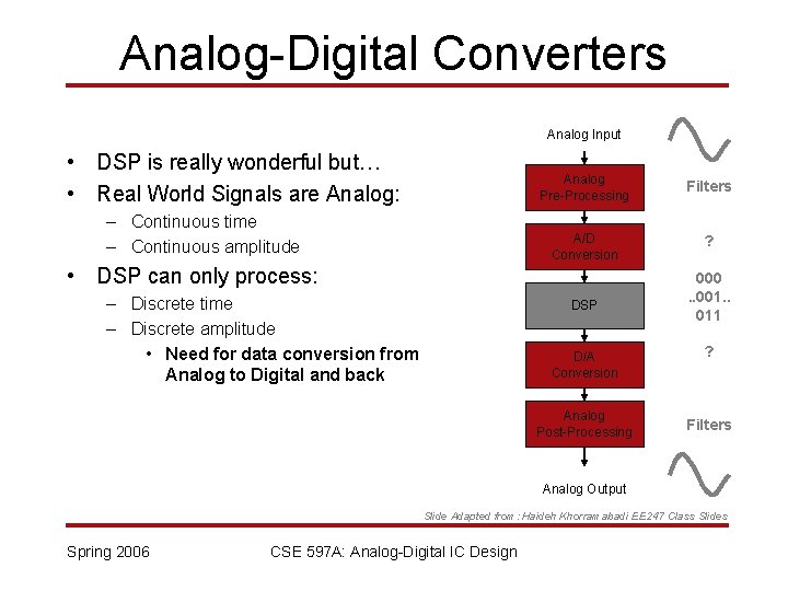
Analog-Digital Converters Analog Input • DSP is really wonderful but… • Real World Signals are Analog: – Continuous time – Continuous amplitude Analog Pre-Processing Filters A/D Conversion ? • DSP can only process: – Discrete time – Discrete amplitude • Need for data conversion from Analog to Digital and back DSP D/A Conversion Analog Post-Processing 000. . 001. . 011 ? Filters Analog Output Slide Adapted from: Haideh Khorramabadi EE 247 Class Slides Spring 2006 CSE 597 A: Analog-Digital IC Design

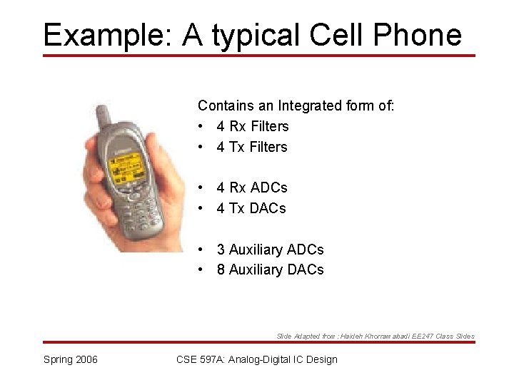
Example: A typical Cell Phone Contains an Integrated form of: • 4 Rx Filters • 4 Tx Filters • 4 Rx ADCs • 4 Tx DACs • 3 Auxiliary ADCs • 8 Auxiliary DACs Slide Adapted from: Haideh Khorramabadi EE 247 Class Slides Spring 2006 CSE 597 A: Analog-Digital IC Design

Flash ADC Spring 2006 CSE 597 A: Analog-Digital IC Design

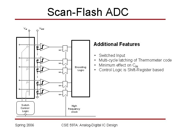
Scan-Flash ADC VIN VREF Additional Features EN EN EN Encoding Logic • • Switched Input Multi-cycle latching of Thermometer code Minimum effect on CIN Control Logic is Shift-Register based EN EN Switch Control Logic Spring 2006 High frequency clock CSE 597 A: Analog-Digital IC Design

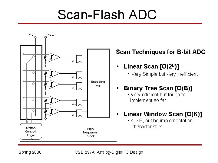
Scan-Flash ADC VIN VREF Scan Techniques for B-bit ADC EN • Linear Scan [O(2 B)] • Very Simple but very inefficient EN EN Encoding Logic • Binary Tree Scan [O(B)] • Very efficient but tough to implement so far EN • Linear Window Scan [O(K)] EN Switch Control Logic Spring 2006 High frequency clock • K > B, but be implementation characteristics CSE 597 A: Analog-Digital IC Design

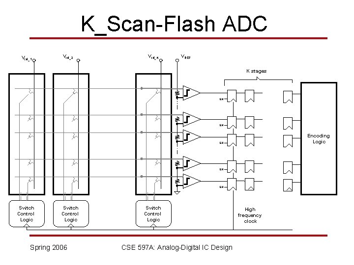
K_Scan-Flash ADC VIN_1 VIN_2 VIN_K VREF K stages EN EN Encoding Logic EN EN EN Switch Control Logic Spring 2006 Switch Control Logic CSE 597 A: Analog-Digital IC Design High frequency clock
![Target Specifications 2 Channels 2 ScanFlash ADC 12 bit per channel Power Target Specifications • • 2 Channels [2 -Scan-Flash ADC] 12 bit per channel Power](https://slidetodoc.com/presentation_image/2370644414ef451b7ea496f869d75355/image-9.jpg)
Target Specifications • • 2 Channels [2 -Scan-Flash ADC] 12 bit per channel Power Supply: 5 V Power Consumption: 400 m. W DNL/INL: 1 LSB Area: 1 mm 2 Speed: 50 MSPS per channel (100 MSPS aggregate) Operating Frequency: 100 MHz Spring 2006 CSE 597 A: Analog-Digital IC Design

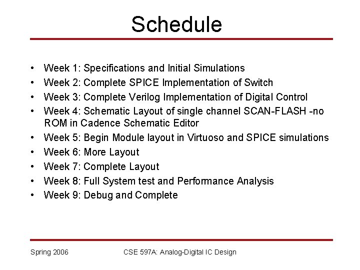
Schedule • • • Week 1: Specifications and Initial Simulations Week 2: Complete SPICE Implementation of Switch Week 3: Complete Verilog Implementation of Digital Control Week 4: Schematic Layout of single channel SCAN-FLASH -no ROM in Cadence Schematic Editor Week 5: Begin Module layout in Virtuoso and SPICE simulations Week 6: More Layout Week 7: Complete Layout Week 8: Full System test and Performance Analysis Week 9: Debug and Complete Spring 2006 CSE 597 A: Analog-Digital IC Design

References Spring 2006 CSE 597 A: Analog-Digital IC Design