RPC Technical Trigger Flavio Loddo I N F
- Slides: 10
RPC Technical Trigger Flavio Loddo I. N. F. N. Bari on behalf of Barrel RPC Collaboration CMS Week 14 -16 March 2005 F. Loddo INFN-Bari
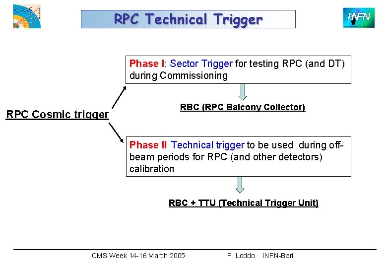
RPC Technical Trigger Phase I: Sector Trigger for testing RPC (and DT) during Commissioning RPC Cosmic trigger RBC (RPC Balcony Collector) Phase II: Technical trigger to be used during offbeam periods for RPC (and other detectors) calibration RBC + TTU (Technical Trigger Unit) CMS Week 14 -16 March 2005 F. Loddo INFN-Bari
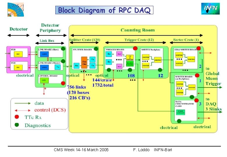
Block Diagram of RPC DAQ CMS Week 14 -16 March 2005 F. Loddo INFN-Bari
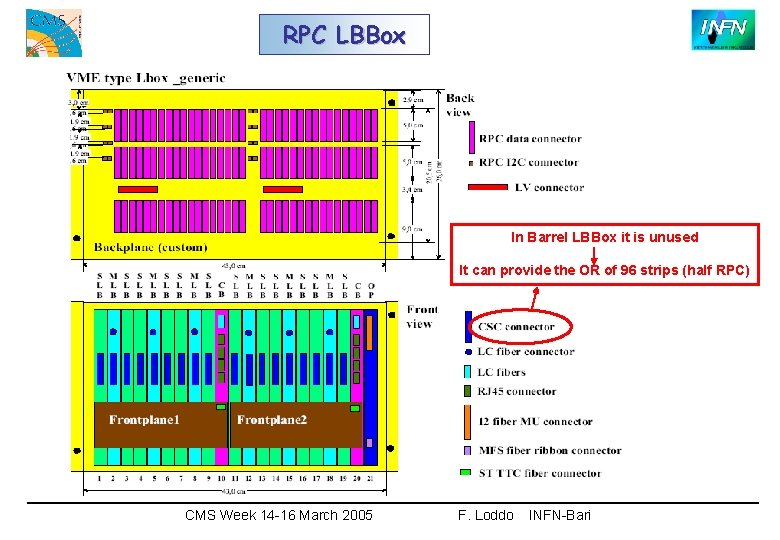
RPC LBBox In Barrel LBBox it is unused It can provide the OR of 96 strips (half RPC) CMS Week 14 -16 March 2005 F. Loddo INFN-Bari
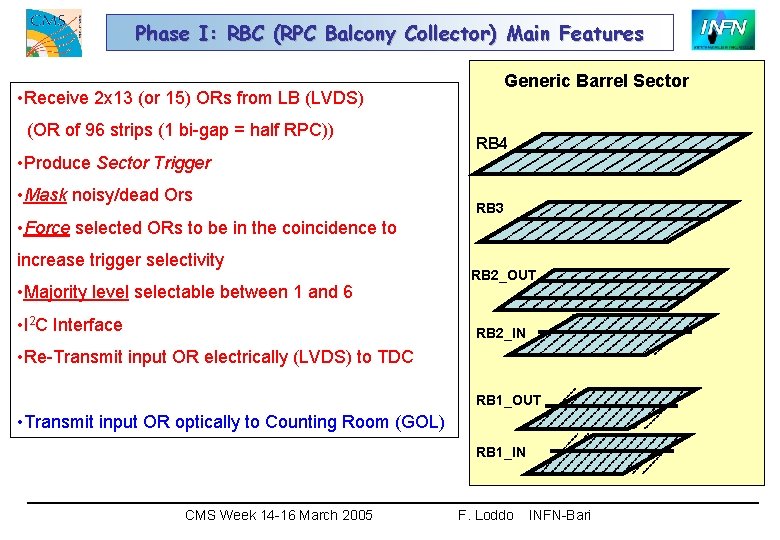
Phase I: RBC (RPC Balcony Collector) Main Features • Receive 2 x 13 (or 15) ORs from LB (LVDS) (OR of 96 strips (1 bi-gap = half RPC)) • Produce Sector Trigger • Mask noisy/dead Ors Generic Barrel Sector RB 4 RB 3 • Force selected ORs to be in the coincidence to increase trigger selectivity • Majority level selectable between 1 and 6 • I 2 C Interface RB 2_OUT RB 2_IN • Re-Transmit input OR electrically (LVDS) to TDC RB 1_OUT • Transmit input OR optically to Counting Room (GOL) RB 1_IN CMS Week 14 -16 March 2005 F. Loddo INFN-Bari
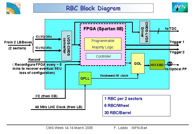
RBC Block Diagram From 2 LBBoxes (2 sectors) 13 (15) ORs LVDS-CMOS converter 13 (15) ORs Programmable CMOS-LVDS Driver FPGA (Spartan IIE) to TDC Trigger 1 Majority Logic Trigger 2 Controller Reconf ( Reconfigure FPGA every ~ 5 mins to recover eventual SEU loss of configuration) GOL HFE 4383 to Optical PP QPLL I 2 C (from CB) 40 MHz LHC Clock (from LB) Deskewed HF clock 1 RBC per 2 sectors 6 RBC/Wheel 30 RBC/Barrel CMS Week 14 -16 March 2005 F. Loddo INFN-Bari
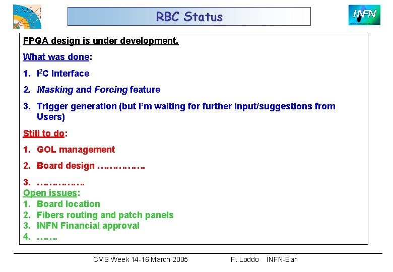
RBC Status FPGA design is under development. What was done: 1. I 2 C Interface 2. Masking and Forcing feature 3. Trigger generation (but I’m waiting for further input/suggestions from Users) Still to do: 1. GOL management 2. Board design ……………. 3. ……………. Open issues: 1. Board location 2. Fibers routing and patch panels 3. INFN Financial approval 4. ……. CMS Week 14 -16 March 2005 F. Loddo INFN-Bari
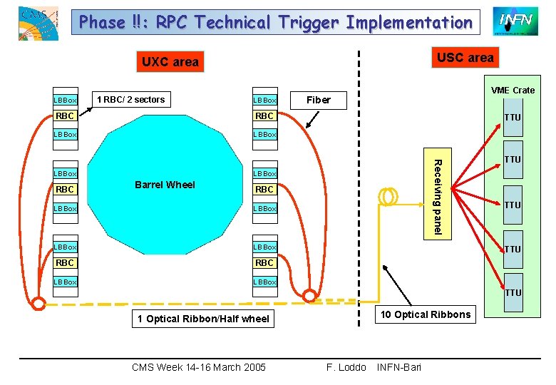
Phase !!: RPC Technical Trigger Implementation USC area UXC area LBBox 1 RBC/ 2 sectors LBBox RBC Fiber TTU Receiving panel LBBox VME Crate LBBox Barrel Wheel RBC LBBox RBC LBBox TTU TTU 10 Optical Ribbons 1 Optical Ribbon/Half wheel CMS Week 14 -16 March 2005 F. Loddo INFN-Bari
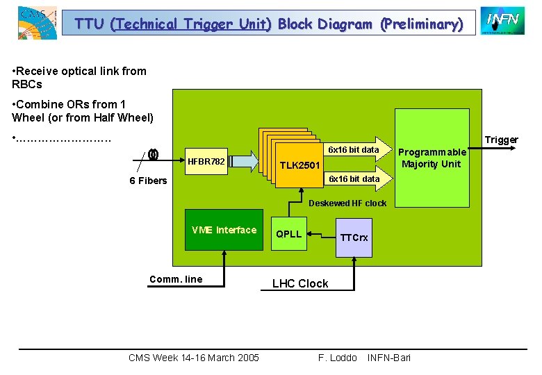
TTU (Technical Trigger Unit) Block Diagram (Preliminary) ( • Receive optical link from RBCs • Combine ORs from 1 Wheel (or from Half Wheel) • …………. . HFBR 782 TLK 2501 TLK 2501 6 x 16 bit data Trigger Programmable Majority Unit 6 x 16 bit data 6 Fibers Deskewed HF clock VME Interface Comm. line CMS Week 14 -16 March 2005 QPLL TTCrx LHC Clock F. Loddo INFN-Bari
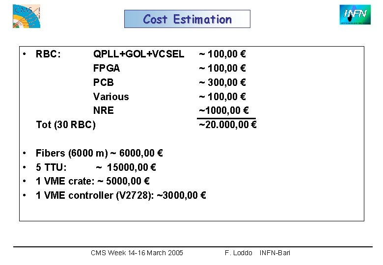
Cost Estimation • RBC: QPLL+GOL+VCSEL FPGA PCB Various NRE Tot (30 RBC) • • ~ 100, 00 € ~ 300, 00 € ~ 100, 00 € ~1000, 00 € ~20. 000, 00 € Fibers (6000 m) ~ 6000, 00 € 5 TTU: ~ 15000, 00 € 1 VME crate: ~ 5000, 00 € 1 VME controller (V 2728): ~3000, 00 € CMS Week 14 -16 March 2005 F. Loddo INFN-Bari