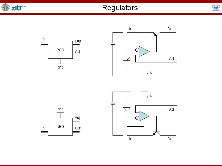
Regulators In In Out POS Adj gnd gnd
- Slides: 8
Regulators In In Out POS Adj gnd gnd Adj In NEG Out In Out 1
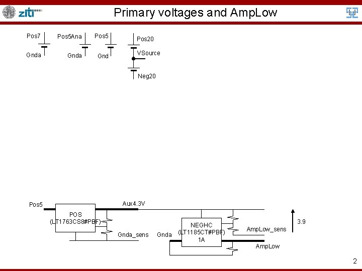
Primary voltages and Amp. Low Pos 7 Pos 5 Ana Pos 5 Gnda Gnd Pos 20 VSource Neg 20 Aux 4. 3 V Pos 5 POS (LT 1763 CS 8#PBF) Gnda_sens Gnda NEGHC (LT 1185 CT#PBF) 1 A 3. 9 Amp. Low_sens Amp. Low 2
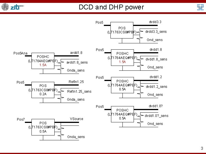
DCD and DHP power dvdd 3. 3 Pos 5 POS (LT 1763 CS 8#PBF) dvdd 3. 3_sens Gnd_sens Pos 5 Ana avdd 1. 8 POSHC (LT 1764 AEQ#PBF) 1. 5 A Pos 5 avdd 1. 8_sens dvdd 1. 8 POSHC (LT 1764 AEQ#PBF) 1. 5 A Gnd_sens Gnda_sens Pos 5 Ref. In 1. 25 POS (LT 1763 CS 8#PBF) 0. 2 A dvdd 1. 8_sens Ref. In 1. 25_sens dvdd 1. 2 POSHC (LT 1764 AEQ#PBF) 0. 5 A dvdd 1. 2_sens Gnda_sens Pos 5 Pos 7 VSource POS (LT 1763 CS 8#PBF) 0. 5 A dvdd 1. 0? POSHC (LT 1764 AEQ#PBF) 0. 5 A dvdd 1. 0? _sens Gnda_sens 3
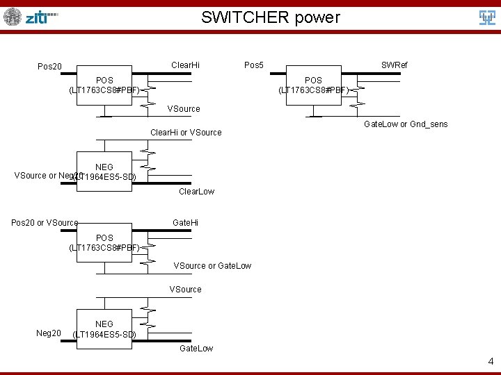
SWITCHER power Clear. Hi Pos 20 SWRef Pos 5 POS (LT 1763 CS 8#PBF) VSource Clear. Hi or VSource Gate. Low or Gnd_sens NEG VSource or Neg 20 (LT 1964 ES 5 -SD) Clear. Low Pos 20 or VSource Gate. Hi POS (LT 1763 CS 8#PBF) VSource or Gate. Low VSource Neg 20 NEG (LT 1964 ES 5 -SD) Gate. Low 4
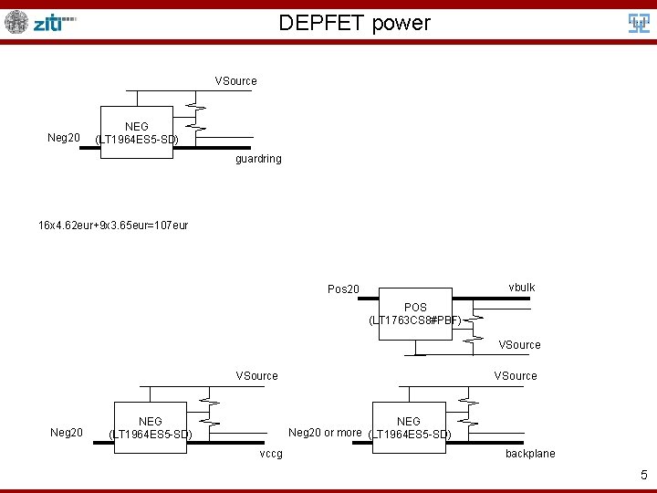
DEPFET power VSource Neg 20 NEG (LT 1964 ES 5 -SD) guardring 16 x 4. 62 eur+9 x 3. 65 eur=107 eur vbulk Pos 20 POS (LT 1763 CS 8#PBF) VSource Neg 20 NEG (LT 1964 ES 5 -SD) VSource NEG Neg 20 or more (LT 1964 ES 5 -SD) vccg backplane 5
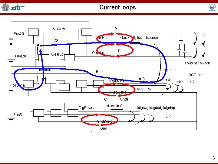
Current loops Clear. Hi A Pos 20 Gate. Hi VSource Neg 20 Clear. Lo <Iac> = 0, Idc = Isource B Gate. Lo Switcher switch Isource E Vdda, Ref. In Pos 5 ana Gnda. Sens C Dig. Power DCD ana Itia Iadc 1, Iadc 2 Amp. Low Gnda <Iac> != 0 Pos 5 Iac = 0 Idigsw, Idigdcd, Idigdhp Dig Gnd. Sens D Gnd 6
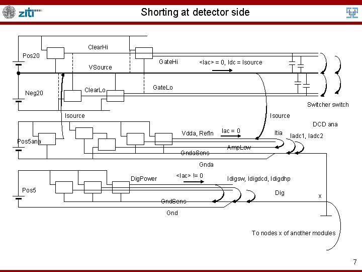
Shorting at detector side Clear. Hi Pos 20 Gate. Hi VSource Neg 20 Clear. Lo <Iac> = 0, Idc = Isource Gate. Lo Switcher switch Isource Vdda, Ref. In Pos 5 ana Gnda. Sens Iac = 0 DCD ana Itia Iadc 1, Iadc 2 Amp. Low Gnda Dig. Power <Iac> != 0 Pos 5 Idigsw, Idigdcd, Idigdhp Dig Gnd. Sens x Gnd To nodes x of another modules 7
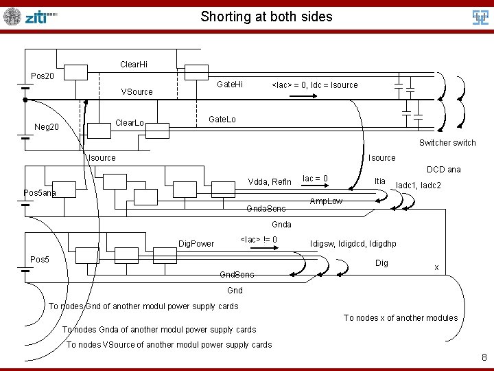
Shorting at both sides Clear. Hi Pos 20 Gate. Hi VSource Neg 20 Clear. Lo <Iac> = 0, Idc = Isource Gate. Lo Switcher switch Isource Vdda, Ref. In Pos 5 ana Gnda. Sens Iac = 0 DCD ana Itia Iadc 1, Iadc 2 Amp. Low Gnda <Iac> != 0 Dig. Power Pos 5 Idigsw, Idigdcd, Idigdhp Dig Gnd. Sens x Gnd To nodes Gnd of another modul power supply cards To nodes x of another modules To nodes Gnda of another modul power supply cards To nodes VSource of another modul power supply cards 8