IO PADS In Out In Out Gnd Vdd

- Slides: 18

I/O PADS In, Out , In. Out , Gnd , Vdd, Source follower

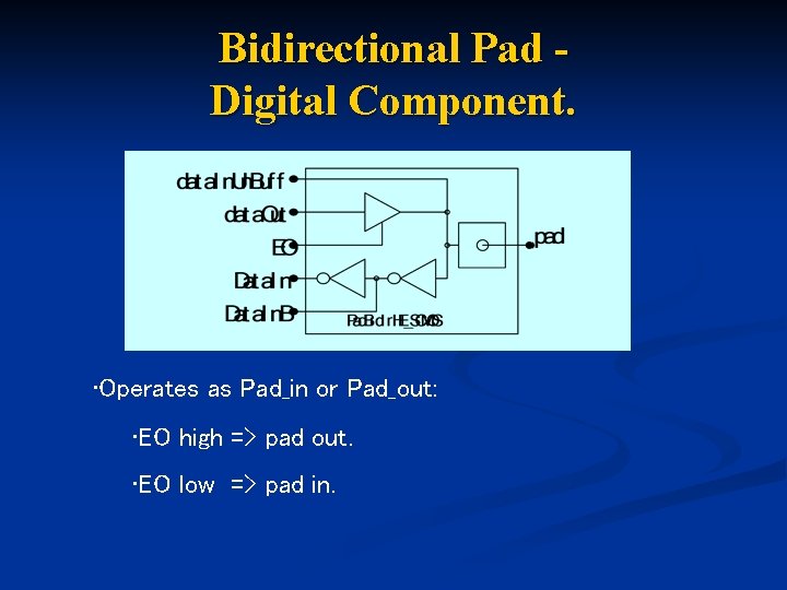
Bidirectional Pad Digital Component. • Operates as Pad_in or Pad_out: • EO high => pad out. • EO low => pad in.

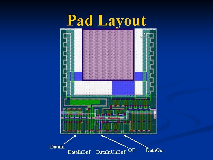
Pad Layout Data. In. Buf Data. In. Un. Buf OE Data. Out

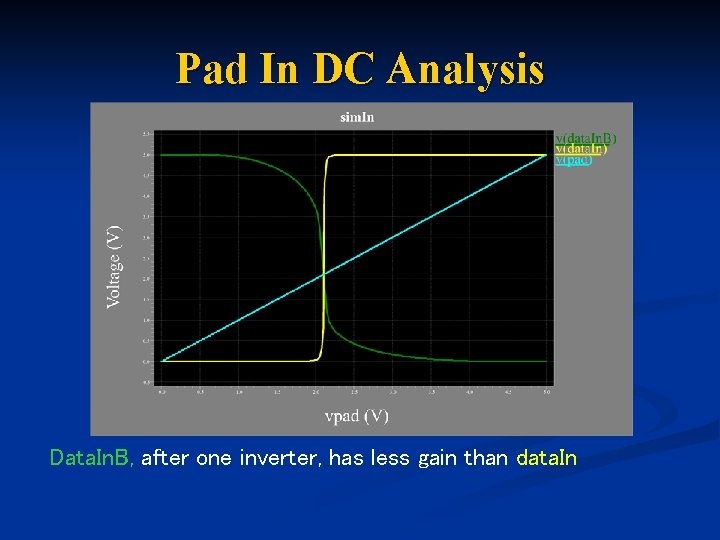
Pad In DC Analysis Data. In. B, after one inverter, has less gain than data. In

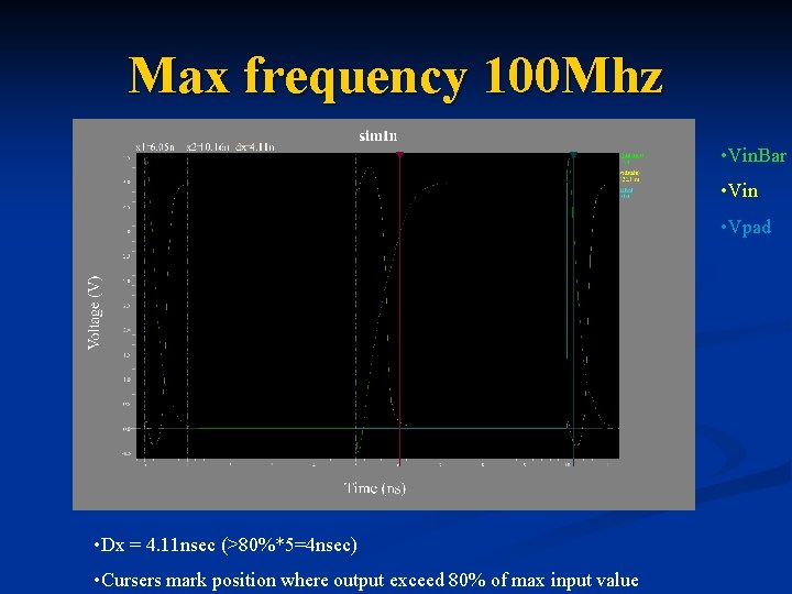
Max frequency 100 Mhz • Vin. Bar • Vin • Vpad • Dx = 4. 11 nsec (>80%*5=4 nsec) • Cursers mark position where output exceed 80% of max input value

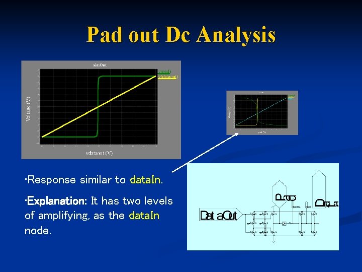
Pad out Dc Analysis • Response similar to data. In. • Explanation: It has two levels of amplifying, as the data. In node.

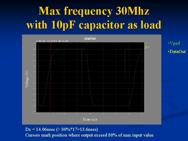
Max frequency 30 Mhz with 10 p. F capacitor as load • Vpad • Data. Out Dx = 14. 06 nsec (> 80%*17=13. 6 nsec) Cursors mark position where output exceed 80% of max input value

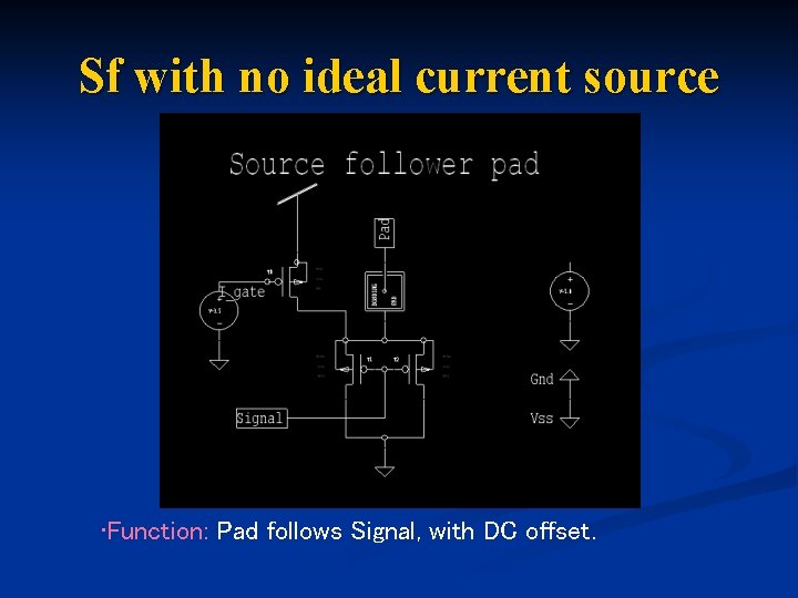
Sf with no ideal current source • Function: Pad follows Signal, with DC offset.

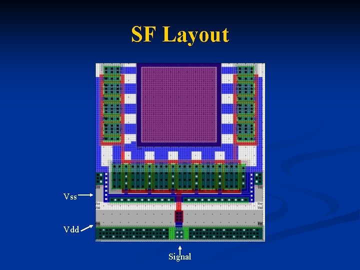
SF Layout Vss Vdd Signal

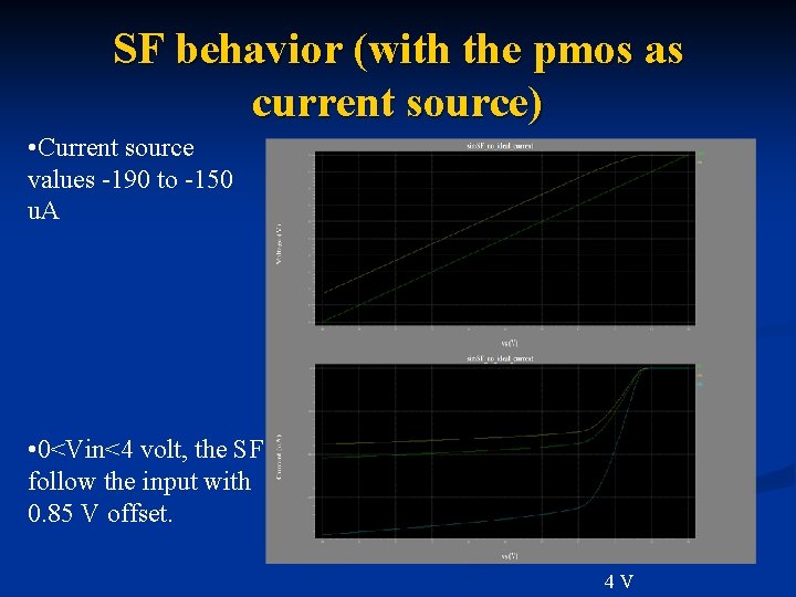
SF behavior (with the pmos as current source) • Current source values -190 to -150 u. A 3. 5 V • 0<Vin<4 volt, the SF follow the input with 0. 85 V offset. 4 V

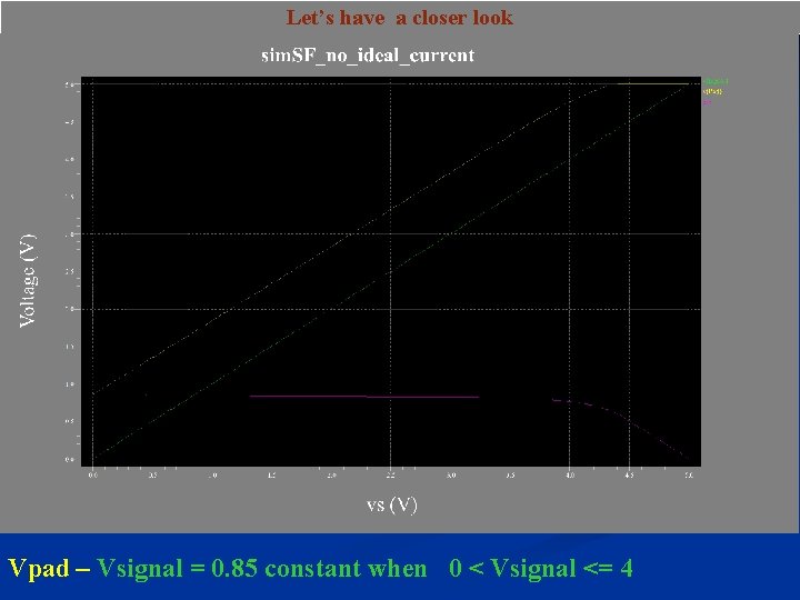
Let’s have a closer look Vpad – Vsignal = 0. 85 constant when 0 < Vsignal <= 4

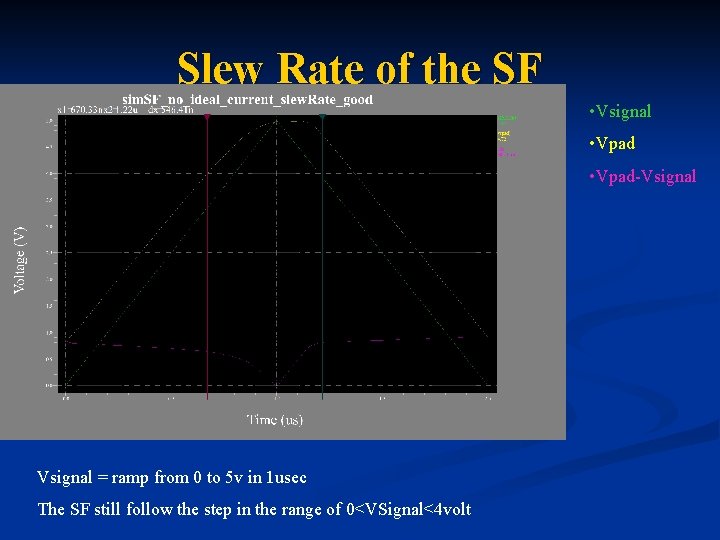
Slew Rate of the SF • Vsignal • Vpad-Vsignal = ramp from 0 to 5 v in 1 usec The SF still follow the step in the range of 0<VSignal<4 volt

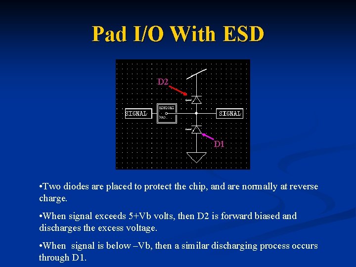
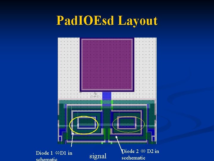
Pad I/O With ESD D 2 D 1 • Two diodes are placed to protect the chip, and are normally at reverse charge. • When signal exceeds 5+Vb volts, then D 2 is forward biased and discharges the excess voltage. • When signal is below –Vb, then a similar discharging process occurs through D 1.

Pad. IOEsd Layout Diode 1 D 1 in signal Diode 2 D 2 in scehematic

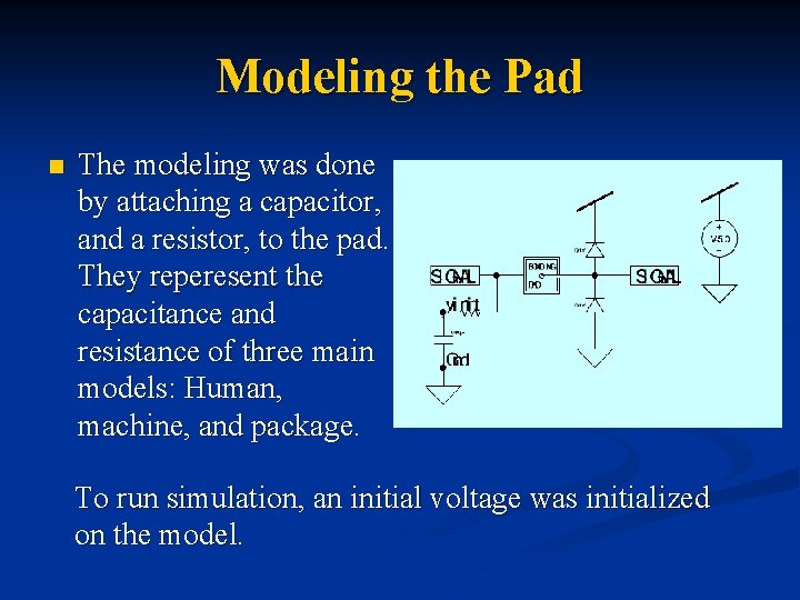
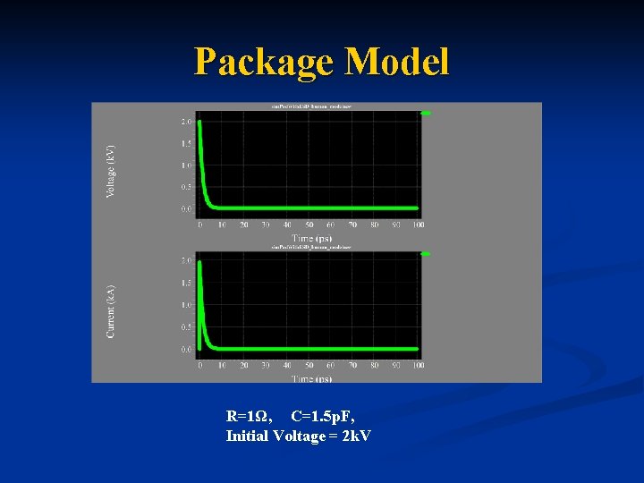
Modeling the Pad n The modeling was done by attaching a capacitor, and a resistor, to the pad. They reperesent the capacitance and resistance of three main models: Human, machine, and package. To run simulation, an initial voltage was initialized on the model.

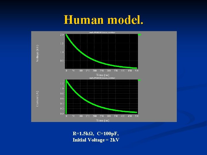
Human model. R=1. 5 kΩ, C=100 p. F, Initial Voltage = 2 k. V

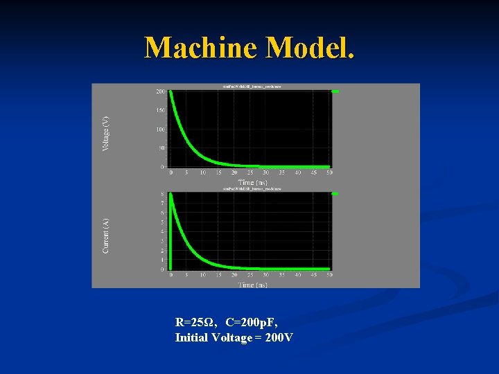
Machine Model. R=25Ω, C=200 p. F, Initial Voltage = 200 V

Package Model R=1Ω, C=1. 5 p. F, Initial Voltage = 2 k. V