Receiver TDP Report to US SKA Consortium May
- Slides: 10

Receiver TDP Report to US SKA Consortium May 22, 2008 Sandy Weinreb, Joe Bardin, Glenn Jones, and Hamdi Mani California Institute of Technology sweinreb@caltech. edu • Work Statement • 2008 Telescope Tests – GAVRT 34 m • Noise Temperature Budget • LNA Status • Feed Integration

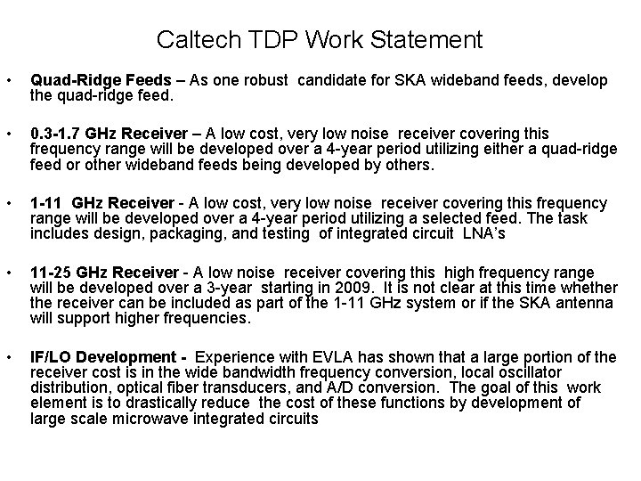
Caltech TDP Work Statement • Quad-Ridge Feeds – As one robust candidate for SKA wideband feeds, develop the quad-ridge feed. • 0. 3 -1. 7 GHz Receiver – A low cost, very low noise receiver covering this frequency range will be developed over a 4 -year period utilizing either a quad-ridge feed or other wideband feeds being developed by others. • 1 -11 GHz Receiver - A low cost, very low noise receiver covering this frequency range will be developed over a 4 -year period utilizing a selected feed. The task includes design, packaging, and testing of integrated circuit LNA’s • 11 -25 GHz Receiver - A low noise receiver covering this high frequency range will be developed over a 3 -year starting in 2009. It is not clear at this time whether the receiver can be included as part of the 1 -11 GHz system or if the SKA antenna will support higher frequencies. • IF/LO Development - Experience with EVLA has shown that a large portion of the receiver cost is in the wide bandwidth frequency conversion, local oscillator distribution, optical fiber transducers, and A/D conversion. The goal of this work element is to drastically reduce the cost of these functions by development of large scale microwave integrated circuits

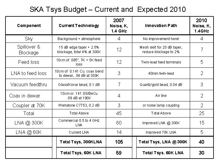
SKA Tsys Budget – Current and Expected 2010 2007 2010 Component Current Technology Noise, K, 1. 4 GHz Innovation Path Noise, K, 1. 4 GHz Sky Background + atmosphere 4 No improvement here! 4 Spillover & Blockage 15 d. B edge taper + 2. 5% blockage, total 4% at 300 K 12 Mesh skirt for 20 d. B taper, reduce blockage to 2% 7 Feed loss 10 cm of. 085”, 7 K + 5 K feed loss 12 Twin-lead feed terminals 5 LNA to feed loss 10 cm of 0. 141 Cu coax bend to dewar, . 04 d. B at 300 K 3 40 mm twin-lead 2 Vacuum feedthru Glass/Kovar bead, 0. 1 d. B 7 Quartz/gold bead, 0. 04 d. B 3 10 cm or. 141 SS/Be. Cu. 09 d. B at 190 K 4 Air line 2 Coupler at 70 K Werlatone C 7753, 0. 2 d. B 3 or noise lamp coupling 2 Total Above 45 Total Above 25 LNA @ 300 K Commercial 0. 5 to 4 GHz LNA 60 Improved LNA @ 300 K 15 LNA @ 60 K Current LNA 14 Improved 70 K LNA 5 Coax in dewar Total Tsys, 300 KLNA 105 Total Tsys, LNA @ 300 K 40 Total Tsys, 60 K LNA 59 Total Tsys. 60 K LNA 30

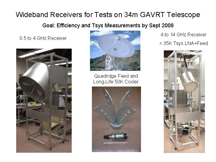
Wideband Receivers for Tests on 34 m GAVRT Telescope Goal: Efficiency and Tsys Measurements by Sept 2008 4 to 14 GHz Receiver 0. 5 to 4 GHz Receiver < 35 K Tsys LNA+Feed Quadridge Feed and Long-Life 50 K Cooler

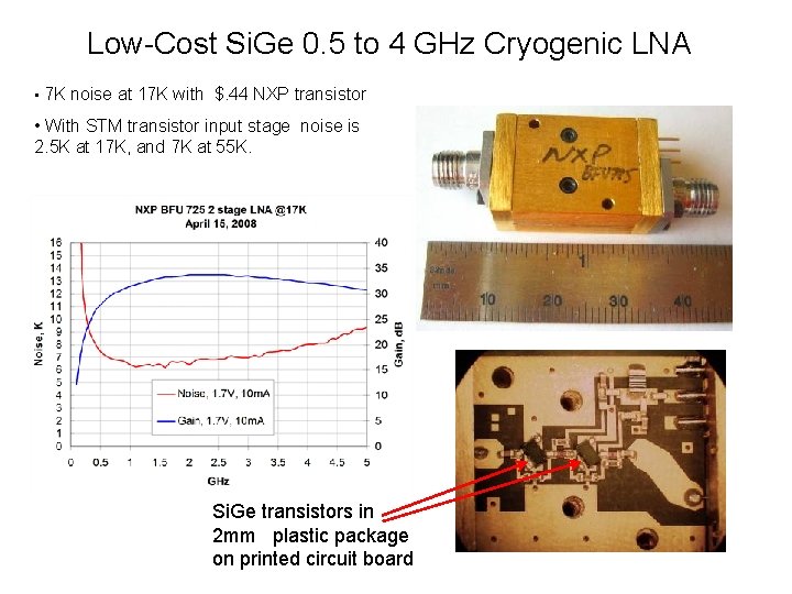
Low-Cost Si. Ge 0. 5 to 4 GHz Cryogenic LNA • 7 K noise at 17 K with $. 44 NXP transistor • With STM transistor input stage noise is 2. 5 K at 17 K, and 7 K at 55 K. Si. Ge transistors in 2 mm plastic package on printed circuit board

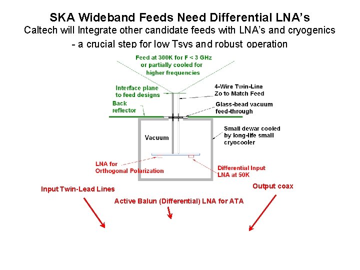
SKA Wideband Feeds Need Differential LNA’s Caltech will Integrate other candidate feeds with LNA’s and cryogenics - a crucial step for low Tsys and robust operation Input Twin-Lead Lines Active Balun (Differential) LNA for ATA Output coax

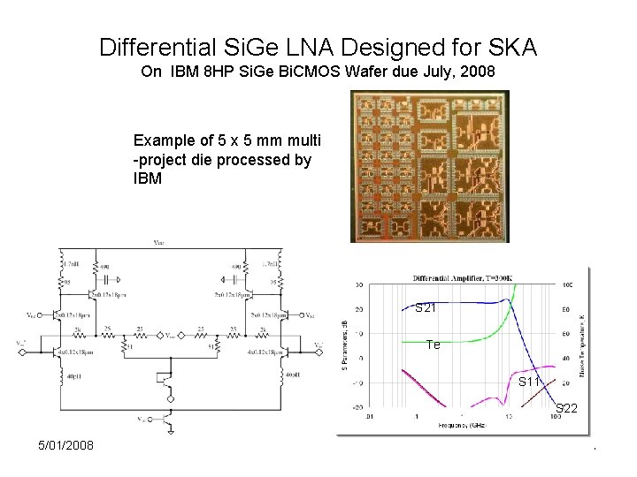
Differential Si. Ge LNA Designed for SKA On IBM 8 HP Si. Ge Bi. CMOS Wafer due July, 2008 Example of 5 x 5 mm multi -project die processed by IBM S 21 Te S 11 S 22 5/01/2008 7

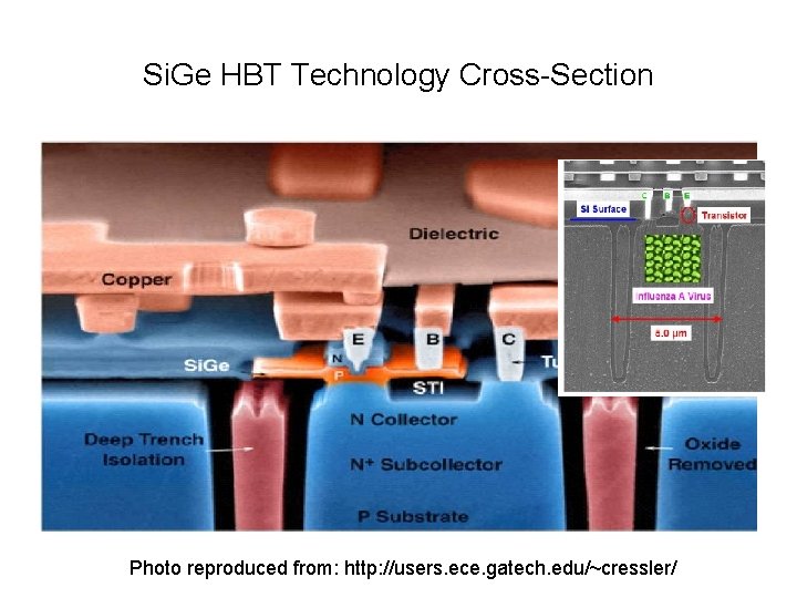
Si. Ge HBT Technology Cross-Section Photo reproduced from: http: //users. ece. gatech. edu/~cressler/

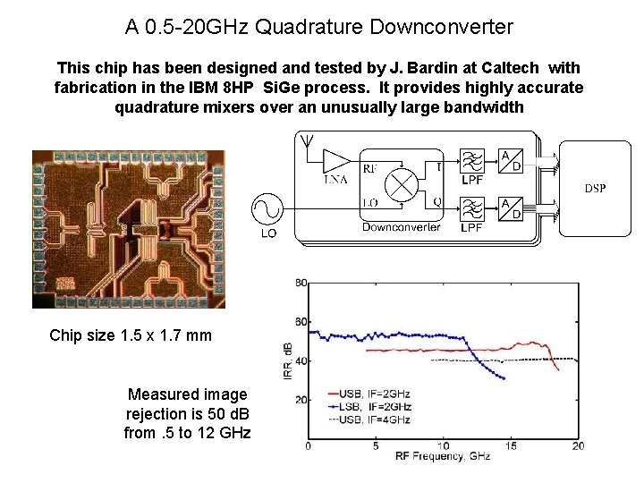
A 0. 5 -20 GHz Quadrature Downconverter This chip has been designed and tested by J. Bardin at Caltech with fabrication in the IBM 8 HP Si. Ge process. It provides highly accurate quadrature mixers over an unusually large bandwidth Chip size 1. 5 x 1. 7 mm Measured image rejection is 50 d. B from. 5 to 12 GHz

Publications and Reports S. Weinreb, J. C. Bardin, and H. Mani, “Design of Cryogenic Si. Ge Low. Noise Amplifiers, ” IEEE Transactions on Microwave Theory and Techniques, Vol. 55, pp. 2306 -2311, Nov. 2007. J. C. Bardin and S. Weinreb, “Experimental Modeling and Noise of Si. Ge HBTs, ” to be published Proc. IEEE International Microwave Symposium, IMS, Atlanta, GA, June 16 -19, 2008. J. C. Bardin and S. Weinreb, “A 0. 5 -20 GHz Quadrature Downconverter, ” to be published IEEE Bipolar/Bi. CMOS Circuits and Technology Meeting, BCTM 2008, Monterey, CA, Oct 13 -16, 2008. For seminars and internal reports see http: //radiometer. caltech. edu