Pinhole test for Time Pix protection layer EKL
- Slides: 3

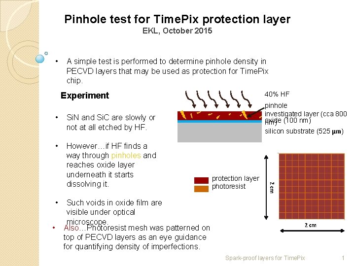
Pinhole test for Time. Pix protection layer EKL, October 2015 • A simple test is performed to determine pinhole density in PECVD layers that may be used as protection for Time. Pix chip. 40% HF Experiment Si. N and Si. C are slowly or not at all etched by HF. • However…if HF finds a way through pinholes and reaches oxide layer underneath it starts dissolving it. • • Such voids in oxide film are visible under optical microscope. Also…Photoresist mesh was patterned on top of PECVD layers as an eye guidance for quantifying density of imperfections. protection layer photoresist 2 cm • pinhole investigated layer (cca 800 oxide nm) (100 nm) silicon substrate (525 μm) 2 cm Spark-proof layers for Time. Pix 1

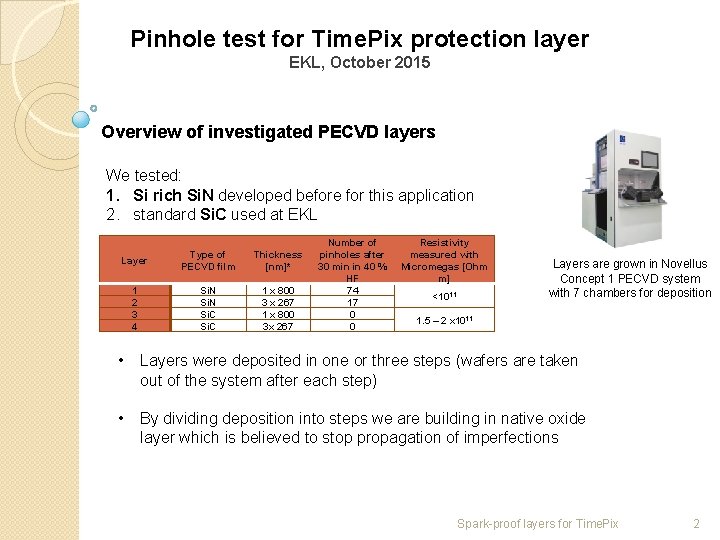
Pinhole test for Time. Pix protection layer EKL, October 2015 Overview of investigated PECVD layers We tested: 1. Si rich Si. N developed before for this application 2. standard Si. C used at EKL Layer Type of PECVD film Thickness [nm]* 1 2 3 4 Si. N Si. C 1 x 800 3 x 267 1 x 800 3 x 267 Number of pinholes after 30 min in 40 % HF 74 17 0 0 Resistivity measured with Micromegas [Ohm m] <1011 Layers are grown in Novellus Concept 1 PECVD system with 7 chambers for deposition 1. 5 – 2 x 10¹¹ • Layers were deposited in one or three steps (wafers are taken out of the system after each step) • By dividing deposition into steps we are building in native oxide layer which is believed to stop propagation of imperfections Spark-proof layers for Time. Pix 2

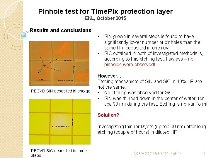
Pinhole test for Time. Pix protection layer EKL, October 2015 Results and conclusions • • PECVD Si. N deposited in one-go Si. N grown in several steps is found to have significantly lower number of pinholes than the same film deposited in one row Si. C obtained in both of investigated methods is, according to this etching test, flawless – no pinholes were observed! However. . . Etching mechanism of Si. N and Si. C in 40% HF are not the same: • No etching was observed for Si. C • Si. N was thinned down in the center of wafer for cca 90 nm during the test. Etching is non-uniform! Solution? Investigating thinner layers (up to 200 nm) after long etching (couple of hours) in diluted HF PECVD Si. C deposited in three steps Spark-proof layers for Time. Pix 3