Time Pix In Grid Problems and solutions Yevgen

Time. Pix / In. Grid Problems and solutions Yevgen Bilevych Amsterdam 28. 01. 2013
 - Silicon nitride -")
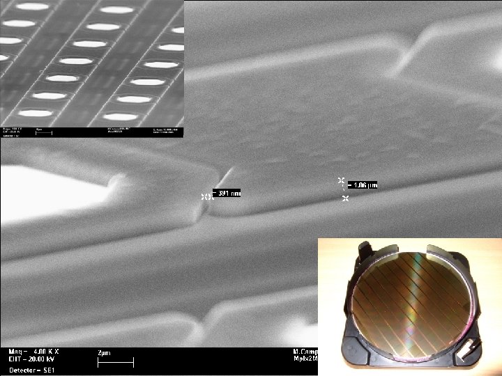
8’’ Time. Pix wafer Surface materials: - Aluminum (aluminum oxide) - Silicon nitride - Silicon oxide 107 single chips Thickness 725 µm

48. 22 mm CHIPEDGE 48. 22 mm 16120 mm Time. Pix chip Pixel Row 255 57. 7 mm 28. 3 mm Pixel Row 254 Pixel Row 253 14111 mm Pixel Row 1 55 mm Pixel Row 0 55 mm 10 mm 20 mm Detector Guard Ring Row 20 mm Snake Top Row CHIPEDGE Column 255 Column 254 Column 253 Column 252 Column 251 Column 4 Column 3 Column 2 Column 1 Column 0 CHIPEDGE 256 x 256 pixels Snake Bottom Row

Main technological steps for the formation of structure Time. Pix / SU-8 / Al grid 1. Formation of protection layer 2. Deposition of spacer material 3. Deposition of the Grid material 4. Formation of structure “support” / grid
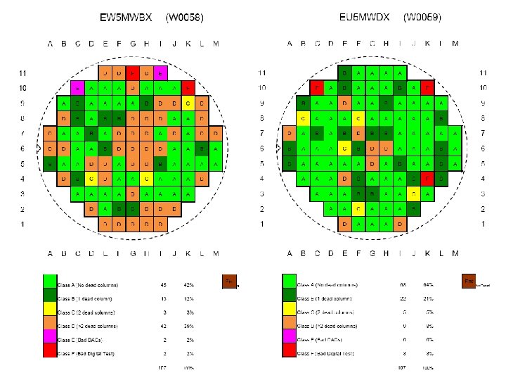

Wafer surface quality inspection W 0058 EW 5 MWBX

Wafer surface quality inspection W 0059 EU 5 MWDX

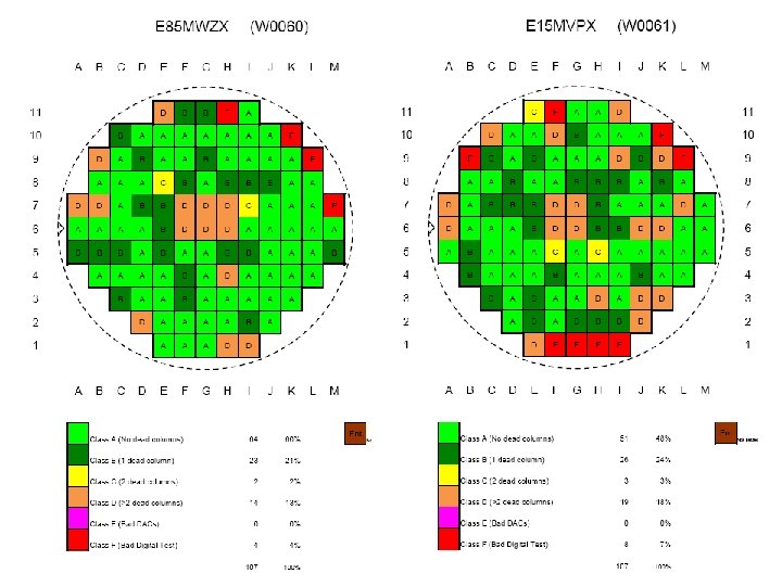
Wafer surface quality inspection W 0060 E 85 MWZX

Wafer surface quality inspection W 0061 E 15 MVPX

Polyimide mask Microsystems HD 4100 polyimide - negative tone, solvent developed, photodefinable polyimide Steps: • Spinning • Baking • Exposition • Development • Silicon nitride deposition • Chemical activation of polyimide • Stripping Advantage: • Silicon technology compatible • Perfect alignment • No residuals Disadvantage: • Temperature sensitive process • Time consuming process • mechanical scratching of bonding pads

PECVD Plasma enhanced chemical vapor deposition Silicone oxide or silicone nitride formation Plasma power max 600 W at 187. 5 k. Hz, max 300 W at 13. 56 MHz plasma frequency Substrate temperature 100 up to 400 °C Layers contain hydrogen Oxford 80 (PECVD)

just deposited Six. Ny “chemically activated polyimide”

SU-8 - epoxy-based negative photoresist SU-8 photoresist composition: - Gamma Butyrolactone 22 -60% - Up to 10 % Triarylsulfonium / Hexafluoroantimonate Salt (3. 3% for SU-8/50) - Propylene Carbonate 1 -5% - Epoxy Resin 35 -75% - C Bisphenol A Novolak epoxy oligomer - O SU-8 crosslinking mechanism O O R 1 CH + H+ CH 2 OH+ R 1 CH CH 2 + R 1 CH - H+ CH 2 O R 1 CH 2 CH CH CH 2 O R 1

SU-8 layer map

Al layer Sputtering system Leybold Z 660 DC 50%, no sputter etching, 30 sec – the deposition time for every sputtering run, + cooling delay Total thickness: ~ 800 nm 1 x 2 x 3 x 4 x 5 x 6 x 7 x 8 x 9 x 10 11 12 13 14 15 16 17 18 19 20 21 22 23 24 25 x x x x

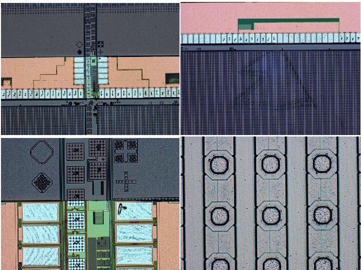
deposition of Al layer Chip Pixel pad protection layer SU-8 photoresist SU-8 column aluminum Cross-linked SU-8 photoresist

Development of SU-8 1. 2. 3. 4. 5. 6. 7. 8. 9. Acetone: IPA: H 2 O (1: 1: 2) Acetone: IPA: H 2 O (1: 1: 1) Acetone: IPA (1: 1) Microstrip 6001 H 2 O IPA Acetone Drying in the air

Standard development

Extra cleaning

O 2 plasma cleaning

O 2 plasma cleaning
")
O 2 plasma cleaning (long time)
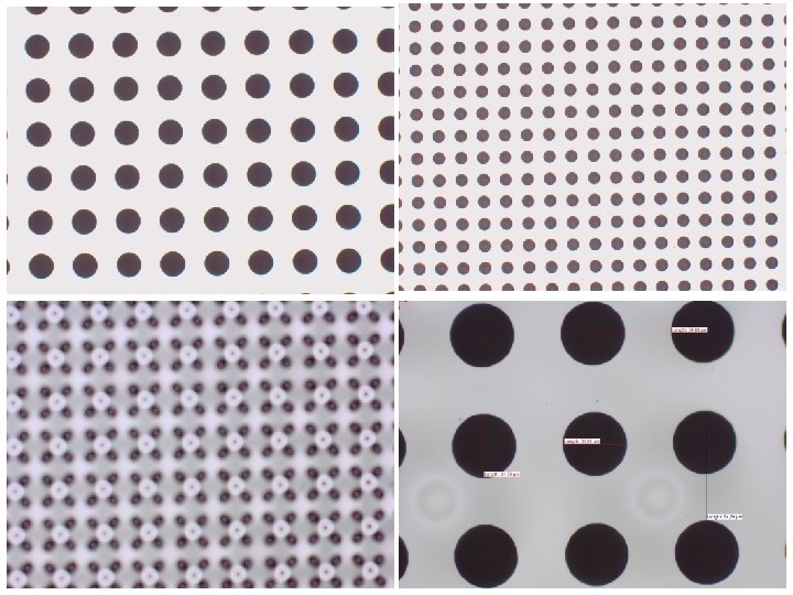

Summary W 0058 EW 5 MWBX (4 mm Si W 0058 EW 5 MWBX ( x. Ny) in process W 0059 EU 5 MWDX (4 mm Si W 0059 ( x. Ny) broken W 0060 E 85 MWZX (8 mm Si W 0060 E 85 MWZX ( x. Ny) in process W 0061 E 15 MVPX (8 mm Si W 0061 E 15 MVPX ( x. Ny) requires the cleaning IZM-5 started: W 0062 (4 mm Six. Ny) and W 0063 (8 mm Six. Ny) Modified In. Grid (m. In. Grid) - started
- Slides: 27