OEICWC Project Task 3 Larry Coldren Leader John
- Slides: 6

OEIC-WC Project Task 3 Larry Coldren, Leader John Bowers, Jeff Henness, Jon Barton, Matt Sysak, James Raring, John Hutchinson (Intel), Hsu-feng Chou With assistance from Dan Blumenthal, Leif Johansson, and Jon Getty University of California Santa Barbara Chip-Scale WDM Program

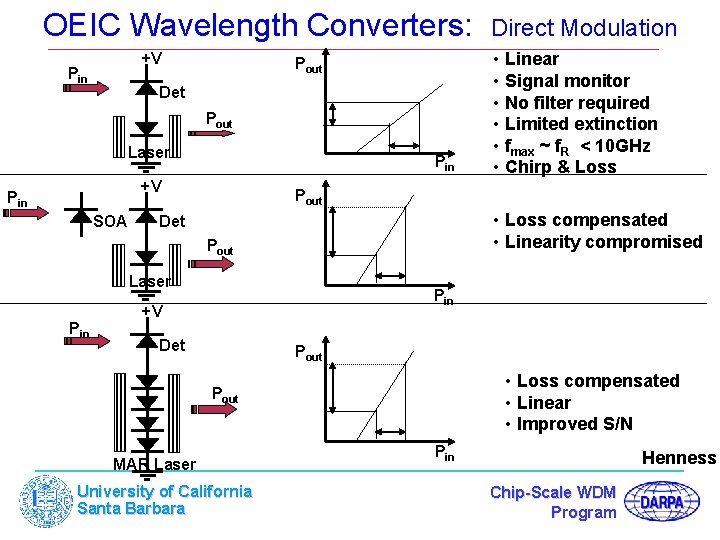
OEIC Wavelength Converters: +V Pin Pout Det Pout Laser Pin +V Pin SOA • Linear • Signal monitor • No filter required • Limited extinction • fmax ~ f. R < 10 GHz • Chirp & Loss Pout • Loss compensated • Linearity compromised Det Pout Laser Pin Direct Modulation Pin +V Det Pout • Loss compensated • Linear • Improved S/N Pout MAR Laser University of California Santa Barbara Pin Henness Chip-Scale WDM Program

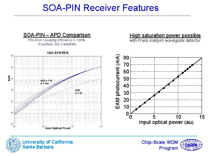
SOA-PIN Receiver Features SOA-PIN – APD Comparison High saturation power possible PIN-SOA Coupling Efficiency = 100% (Courtesy Joe Campbell) EAM photocurrent (m. A) with Franz-Keldysh waveguide detector University of California Santa Barbara 80 70 60 50 40 30 20 10 0 0 5 10 Input optical power (au) Chip-Scale WDM Program 15

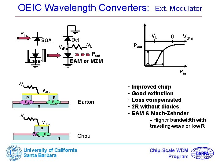
OEIC Wavelength Converters: Pin Det SOA Vd/m Ext. Modulator -Vb 0 Vd/m Pout EAM or MZM Laser Pin -Vb Vd/m p Pdet p Pmod n Barton -Vb Vd/m p Pdet Pmod • Improved chirp • Good extinction • Loss compensated • 2 R without diodes • EAM & Mach-Zehnder - Higher bandwidth with traveling-wave or low R n University of California Santa Barbara Chou Chip-Scale WDM Program

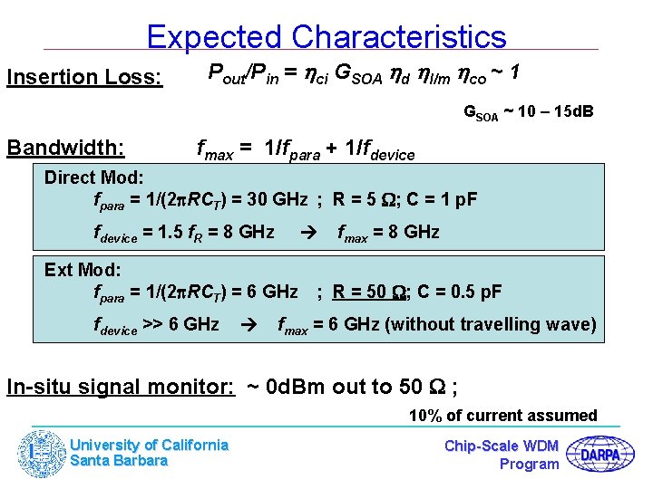
Expected Characteristics Insertion Loss: Pout/Pin = hci GSOA hd hl/m hco ~ 1 GSOA ~ 10 – 15 d. B Bandwidth: fmax = 1/fpara + 1/fdevice Direct Mod: fpara = 1/(2 p. RCT) = 30 GHz ; R = 5 W; C = 1 p. F fdevice = 1. 5 f. R = 8 GHz Ext Mod: fpara = 1/(2 p. RCT) = 6 GHz fdevice >> 6 GHz fmax = 8 GHz ; R = 50 W; C = 0. 5 p. F fmax = 6 GHz (without travelling wave) In-situ signal monitor: ~ 0 d. Bm out to 50 W ; 10% of current assumed University of California Santa Barbara Chip-Scale WDM Program

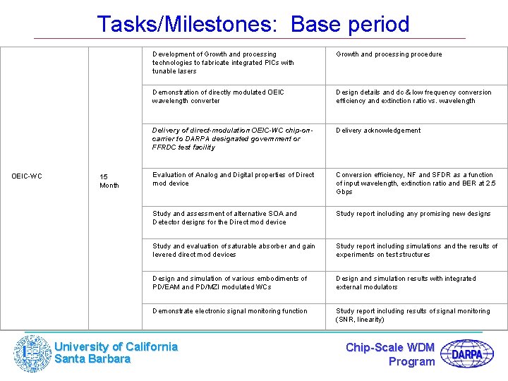
Tasks/Milestones: Base period OEIC-WC 15 Month Development of Growth and processing technologies to fabricate integrated PICs with tunable lasers Growth and processing procedure Demonstration of directly modulated OEIC wavelength converter Design details and dc & low frequency conversion efficiency and extinction ratio vs. wavelength Delivery of direct-modulation OEIC-WC chip-oncarrier to DARPA designated government or FFRDC test facility Delivery acknowledgement Evaluation of Analog and Digital properties of Direct mod device Conversion efficiency, NF and SFDR as a function of input wavelength, extinction ratio and BER at 2. 5 Gbps Study and assessment of alternative SOA and Detector designs for the Direct mod device Study report including any promising new designs Study and evaluation of saturable absorber and gain levered direct mod devices Study report including simulations and the results of experiments on test structures Design and simulation of various embodiments of PD/EAM and PD/MZI modulated WCs Design and simulation results with integrated external modulators Demonstrate electronic signal monitoring function Study report including results of signal monitoring (SNR, linearity) University of California Santa Barbara Chip-Scale WDM Program