My research topics related to surface plasmon Topic

![Super-Lambertian Limit [E. A. Schiff et al. , JAP, (2011)] [M. C. Dennis. et Super-Lambertian Limit [E. A. Schiff et al. , JAP, (2011)] [M. C. Dennis. et](https://slidetodoc.com/presentation_image_h/1139a6b2b1b6b50f81d1bb2e9127d8ee/image-9.jpg)
![Symmetry-breaking in periodic nanostructures by wet etching on Si surfaces Arrows indicate [110] direction Symmetry-breaking in periodic nanostructures by wet etching on Si surfaces Arrows indicate [110] direction](https://slidetodoc.com/presentation_image_h/1139a6b2b1b6b50f81d1bb2e9127d8ee/image-12.jpg)
- Slides: 24

My research topics related to surface plasmon Topic I Manufacturable Symmetry Control in Nanophotonic Light. Trapping Structures to Surpass the Lambertian Limit Topic II Hot electron detector

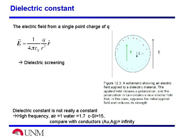
Dielectric constant The electric field from a single point charge of q Dielectric screening Dielectric constant is not really a constant High frequency, air =1 water =1. 7 c-Si=15, compare with conductors (Au, Ag)= infinity

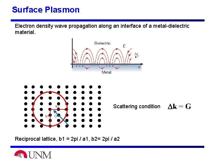
Surface Plasmon Electron density wave propagation along an interface of a metal-dielectric material. k 2 k 1 Scattering condition G Reciprocal lattice, b 1 = 2 pi / a 1, b 2= 2 pi / a 2

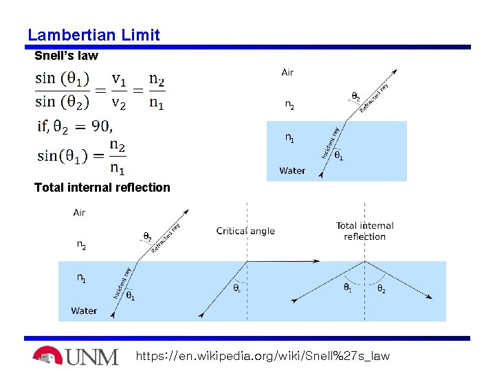
Lambertian Limit Snell’s law Total internal reflection https: //en. wikipedia. org/wiki/Snell%27 s_law

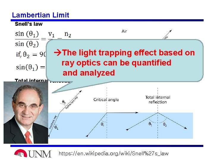
Lambertian Limit Snell’s law The light trapping effect based on ray optics can be quantified analyzed Total internal reflection https: //en. wikipedia. org/wiki/Snell%27 s_law

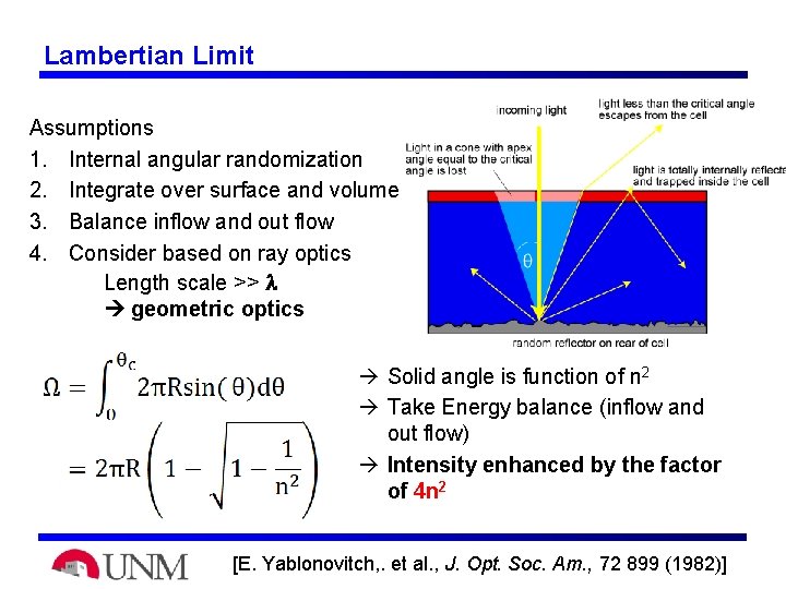
Lambertian Limit Assumptions 1. Internal angular randomization 2. Integrate over surface and volume 3. Balance inflow and out flow 4. Consider based on ray optics Length scale >> l geometric optics Solid angle is function of n 2 Take Energy balance (inflow and out flow) Intensity enhanced by the factor of 4 n 2 [E. Yablonovitch, . et al. , J. Opt. Soc. Am. , 72 899 (1982)]

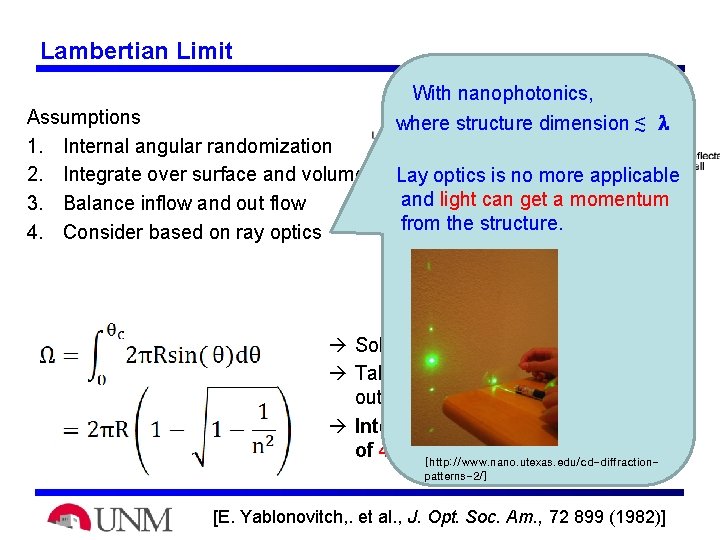
Lambertian Limit Assumptions 1. Internal angular randomization 2. Integrate over surface and volume 3. Balance inflow and out flow 4. Consider based on ray optics With nanophotonics, where structure dimension < ~ l Lay optics is no more applicable and light can get a momentum from the structure. Solid angle is function of n 2 Take Energy balance (inflow and out flow) Intensity enhanced by the factor of 4 n 2 [http: //www. nano. utexas. edu/cd-diffractionpatterns-2/] [E. Yablonovitch, . et al. , J. Opt. Soc. Am. , 72 899 (1982)]

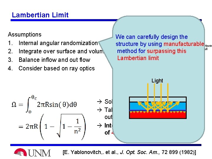
Lambertian Limit Assumptions 1. Internal angular randomization 2. Integrate over surface and volume 3. Balance inflow and out flow 4. Consider based on ray optics We can carefully design the structure by using manufacturable method for surpassing this Lambertian limit Light Solid angle is function of n 2 Take Energy balance (inflow and out flow) Intensity enhanced by the factor of 4 n 2 [E. Yablonovitch, . et al. , J. Opt. Soc. Am. , 72 899 (1982)]
![SuperLambertian Limit E A Schiff et al JAP 2011 M C Dennis et Super-Lambertian Limit [E. A. Schiff et al. , JAP, (2011)] [M. C. Dennis. et](https://slidetodoc.com/presentation_image_h/1139a6b2b1b6b50f81d1bb2e9127d8ee/image-9.jpg)
Super-Lambertian Limit [E. A. Schiff et al. , JAP, (2011)] [M. C. Dennis. et al. , Nano Lett, (2012)] Plasmonic resonator [Z. Yu. et al. , PNAS (2015)] High index guided mode [D. Zhou. et al. , JAP, (2008)] Light trapping limit with SPPs Diffraction grating

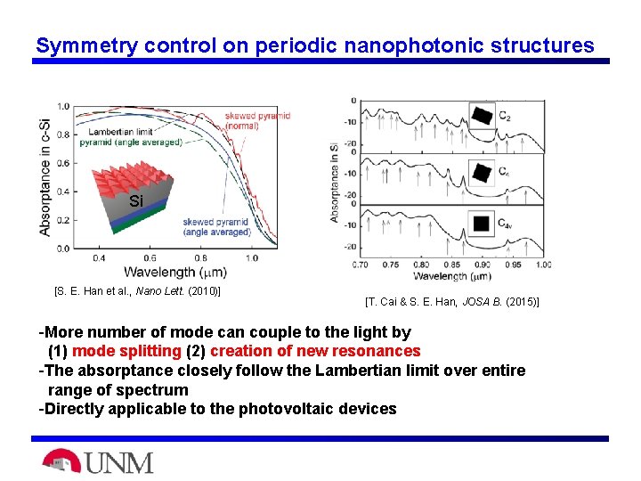
Symmetry control on periodic nanophotonic structures Si [S. E. Han et al. , Nano Lett. (2010)] [T. Cai & S. E. Han, JOSA B. (2015)] -More number of mode can couple to the light by (1) mode splitting (2) creation of new resonances -The absorptance closely follow the Lambertian limit over entire range of spectrum -Directly applicable to the photovoltaic devices

Objective Lambertian limit can be exceeded in nanophotonic regime However, it has not been demonstrated how to integrate the super-lambertian scheme into practical photovoltaic devices Present research will focus on, 1. Manufacturable, cost-effective fabrication of nanophotonic structures 2. Exceeding the Lambertian limit by symmetry breaking of plasmonic structures 3. Directly applicable to photovoltaic devices
![Symmetrybreaking in periodic nanostructures by wet etching on Si surfaces Arrows indicate 110 direction Symmetry-breaking in periodic nanostructures by wet etching on Si surfaces Arrows indicate [110] direction](https://slidetodoc.com/presentation_image_h/1139a6b2b1b6b50f81d1bb2e9127d8ee/image-12.jpg)
Symmetry-breaking in periodic nanostructures by wet etching on Si surfaces Arrows indicate [110] direction of c-Si Misaligning etch mask w. r. t. the c-Si [110] Expected structures after etching and mask removal Experimental structures

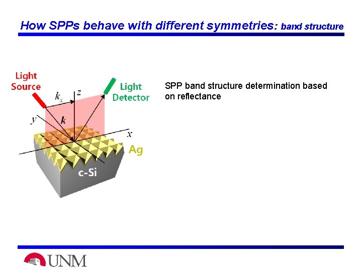
How SPPs behave with different symmetries: band structure SPP band structure determination based on reflectance

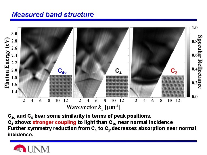
Measured band structure C 4 v and C 4 bear some similarity in terms of peak positions. C 4 shows stronger coupling to light than C 4 v near normal incidence Further symmetry reduction from C 4 to C 2, decreases absorption near normal incidence.

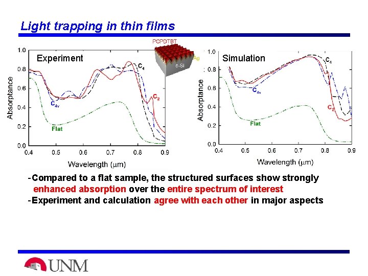
Light trapping in thin films Experiment Simulation -Compared to a flat sample, the structured surfaces show strongly enhanced absorption over the entire spectrum of interest -Experiment and calculation agree with each other in major aspects

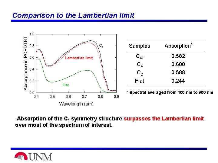
Comparison to the Lambertian limit Samples Absorption* C 4 v C 4 0. 582 0. 600 C 2 0. 588 Flat 0. 244 * Spectral averaged from 400 nm to 900 nm -Absorption of the C 4 symmetry structure surpasses the Lambertian limit over most of the spectrum of interest.

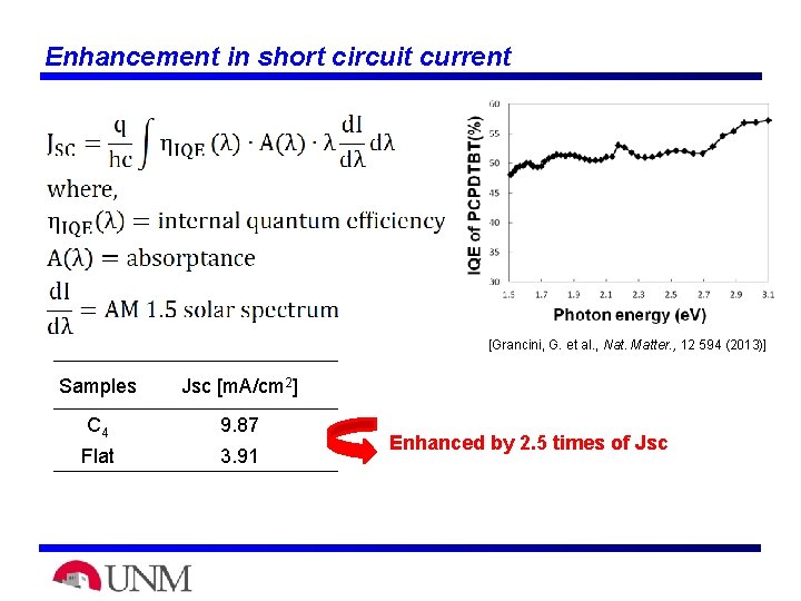
Enhancement in short circuit current [Grancini, G. et al. , Nat. Matter. , 12 594 (2013)] Samples Jsc [m. A/cm 2] C 4 9. 87 Flat 3. 91 Enhanced by 2. 5 times of Jsc

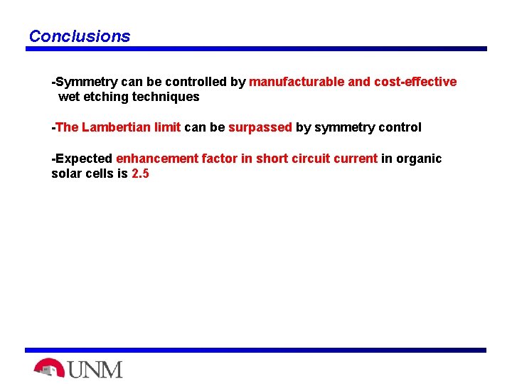
Conclusions -Symmetry can be controlled by manufacturable and cost-effective wet etching techniques -The Lambertian limit can be surpassed by symmetry control -Expected enhancement factor in short circuit current in organic solar cells is 2. 5

My research topics related to surface plasmon Topic I Manufacturable Symmetry Control in Nanophotonic Light. Trapping Structures to Surpass the Lambertian Limit Topic II Hot electron detector

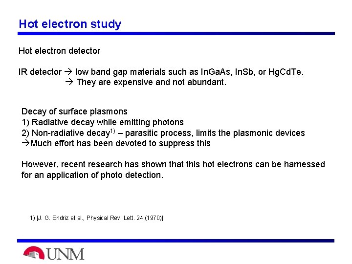
Hot electron study Hot electron detector IR detector low band gap materials such as In. Ga. As, In. Sb, or Hg. Cd. Te. They are expensive and not abundant. Decay of surface plasmons 1) Radiative decay while emitting photons 1) 2) Non-radiative decay – parasitic process, limits the plasmonic devices Much effort has been devoted to suppress this However, recent research has shown that this hot electrons can be harnessed for an application of photo detection. 1) [J. G. Endriz et al. , Physical Rev. Lett. 24 (1970)]

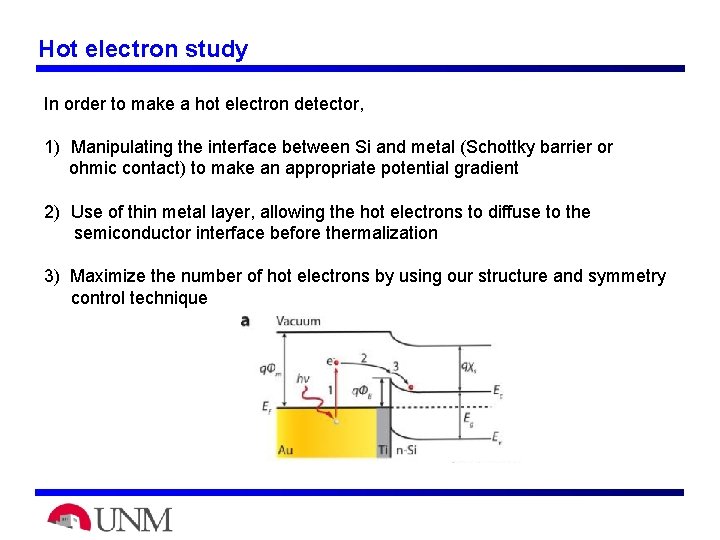
Hot electron study In order to make a hot electron detector, 1) Manipulating the interface between Si and metal (Schottky barrier or ohmic contact) to make an appropriate potential gradient 2) Use of thin metal layer, allowing the hot electrons to diffuse to the semiconductor interface before thermalization 3) Maximize the number of hot electrons by using our structure and symmetry control technique

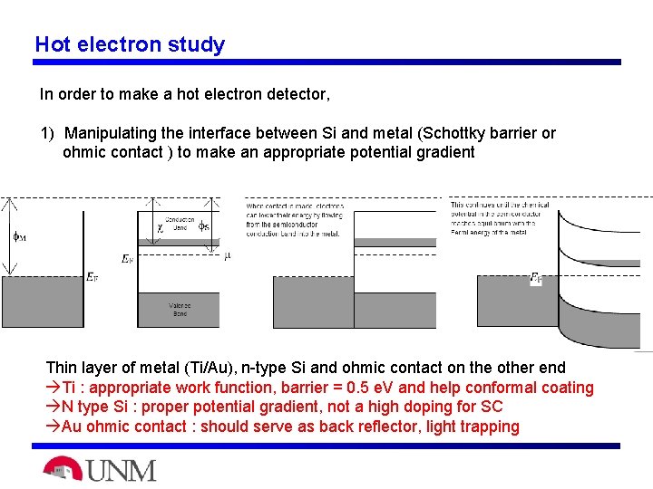
Hot electron study In order to make a hot electron detector, 1) Manipulating the interface between Si and metal (Schottky barrier or ohmic contact ) to make an appropriate potential gradient Thin layer of metal (Ti/Au), n-type Si and ohmic contact on the other end Ti : appropriate work function, barrier = 0. 5 e. V and help conformal coating N type Si : proper potential gradient, not a high doping for SC Au ohmic contact : should serve as back reflector, light trapping

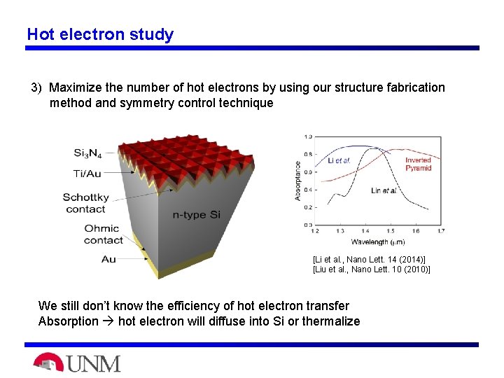
Hot electron study 3) Maximize the number of hot electrons by using our structure fabrication method and symmetry control technique [Li et al. , Nano Lett. 14 (2014)] [Liu et al. , Nano Lett. 10 (2010)] We still don’t know the efficiency of hot electron transfer Absorption hot electron will diffuse into Si or thermalize

Hot electron study: Characterization DROK® High Accuracy 5 Digits Amperage Measure Milli ammeters +/-0 -1. 9999 m. A Digital Current Meter DROK® High Accuracy 2 V Digital Voltmeter +/-0 -1. 9999 V Red LED Voltage Tester 0. 001 V Resolution VOC = 0. 35 e. V Require an IR source