Lecture 13 Announcements You should now purchase the
- Slides: 17
Lecture #13 Announcements • You should now purchase the reader EECS 40: Introduction to Microelectronics, containing reference material from texts by Howe and Sodini and by Rabaey et al. , at Copy Central at Hearst near Euclid Avenue. OUTLINE – Propagation delay – Energy consumption of simple RC circuit – RC circuit transient response examples Reading Start reading Howe & Sodini Ch. 2. 1 -2. 4. 1 EECS 40, Fall 2004 Lecture 13, Slide 1 Prof. White
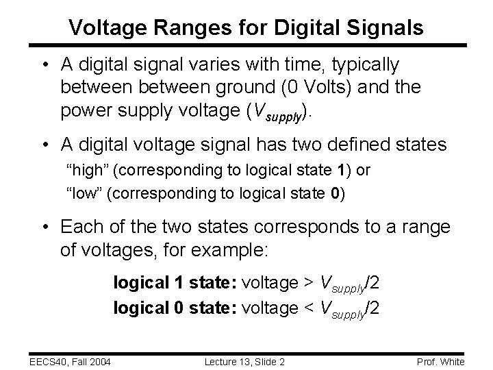
Voltage Ranges for Digital Signals • A digital signal varies with time, typically between ground (0 Volts) and the power supply voltage (Vsupply). • A digital voltage signal has two defined states “high” (corresponding to logical state 1) or “low” (corresponding to logical state 0) • Each of the two states corresponds to a range of voltages, for example: logical 1 state: voltage > Vsupply/2 logical 0 state: voltage < Vsupply/2 EECS 40, Fall 2004 Lecture 13, Slide 2 Prof. White
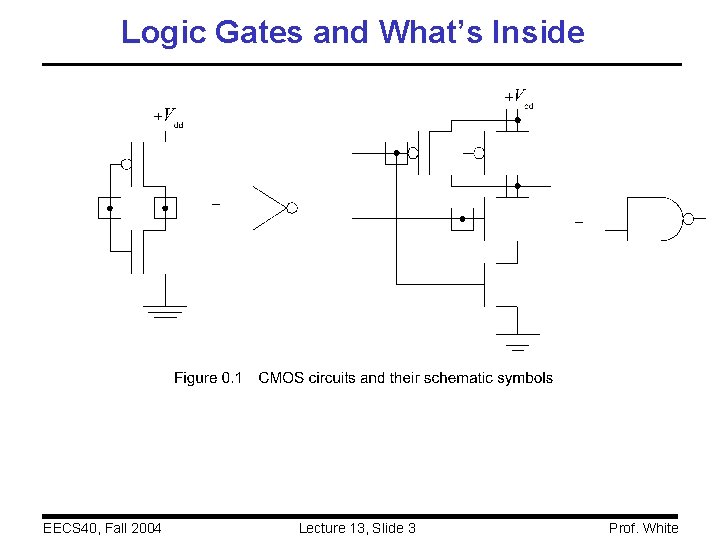
Logic Gates and What’s Inside EECS 40, Fall 2004 Lecture 13, Slide 3 Prof. White
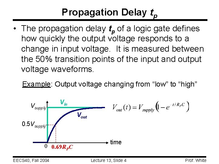
Propagation Delay tp • The propagation delay tp of a logic gate defines how quickly the output voltage responds to a change in input voltage. It is measured between the 50% transition points of the input and output voltage waveforms. Example: Output voltage changing from “low” to “high” Vsupply Vin Vout 0. 5 Vsupply 0 0. 69 RPC EECS 40, Fall 2004 time Lecture 13, Slide 4 Prof. White
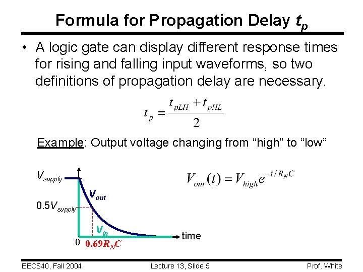
Formula for Propagation Delay tp • A logic gate can display different response times for rising and falling input waveforms, so two definitions of propagation delay are necessary. Example: Output voltage changing from “high” to “low” Vsupply 0. 5 Vsupply Vout Vin 0 0. 69 RNC EECS 40, Fall 2004 time Lecture 13, Slide 5 Prof. White
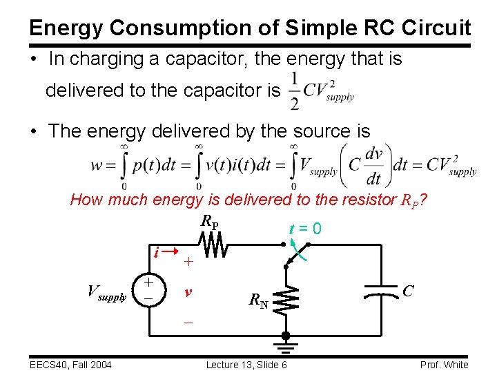
Energy Consumption of Simple RC Circuit • In charging a capacitor, the energy that is delivered to the capacitor is • The energy delivered by the source is How much energy is delivered to the resistor RP? RP t=0 i Vsupply + + v RN C – EECS 40, Fall 2004 Lecture 13, Slide 6 Prof. White
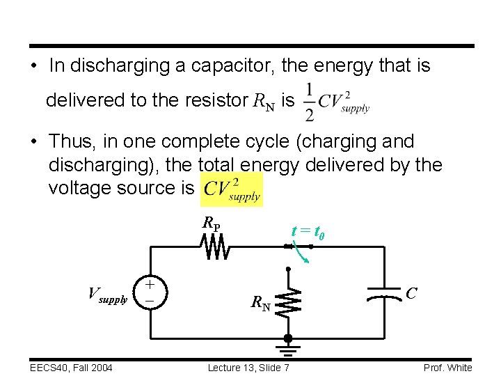
• In discharging a capacitor, the energy that is delivered to the resistor RN is • Thus, in one complete cycle (charging and discharging), the total energy delivered by the voltage source is RP Vsupply EECS 40, Fall 2004 + t = t 0 RN Lecture 13, Slide 7 C Prof. White
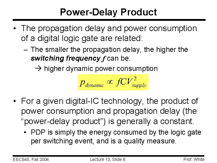
Power-Delay Product • The propagation delay and power consumption of a digital logic gate are related: – The smaller the propagation delay, the higher the switching frequency f can be. à higher dynamic power consumption • For a given digital-IC technology, the product of power consumption and propagation delay (the “power-delay product”) is generally a constant. • PDP is simply the energy consumed by the logic gate per switching event, and is a quality measure. EECS 40, Fall 2004 Lecture 13, Slide 8 Prof. White
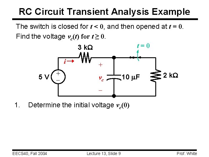
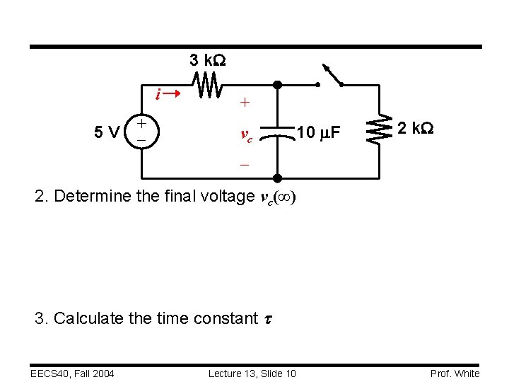
RC Circuit Transient Analysis Example The switch is closed for t < 0, and then opened at t = 0. Find the voltage vc(t) for t ≥ 0. t=0 3 k. W i 5 V + + vc 10 m. F 2 k. W – 1. Determine the initial voltage vc(0) EECS 40, Fall 2004 Lecture 13, Slide 9 Prof. White
3 k. W i 5 V + + vc 10 m. F 2 k. W – 2. Determine the final voltage vc(∞) 3. Calculate the time constant t EECS 40, Fall 2004 Lecture 13, Slide 10 Prof. White
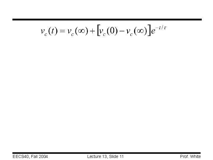
EECS 40, Fall 2004 Lecture 13, Slide 11 Prof. White
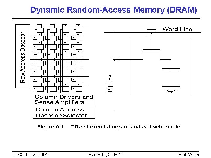
Device Example: Dynamic Random-Access Memory (DRAM) Random-access memory (RAM): array of thousands of memory elements (cells) that store computer instructions and data. Any cell can be accessed in a single operational cycle. The simpler and thus denser random-access memory, dynamic random-access memory or DRAM, uses a single transistor and a capacitor to form the memory cell (see next slide). The transistor acts as a switch to connect the capacitor to the column, or bit line when the row, or word line has a high voltage on it. The capacitor stores charge to indicate a 1. When the switches for a row are closed, the charge on a capacitor that is storing a 1 will cause a voltage rise on the corresponding column wire. A sense amplifier on each column amplifies the small voltage change back to digital levels. Each cell must be refreshed frequently because (a) the reading action diminishes the charges stored on the capacitors, as does (b) leakage in the capacitors. EECS 40, Fall 2004 Lecture 13, Slide 12 Prof. White
Dynamic Random-Access Memory (DRAM) EECS 40, Fall 2004 Lecture 13, Slide 13 Prof. White
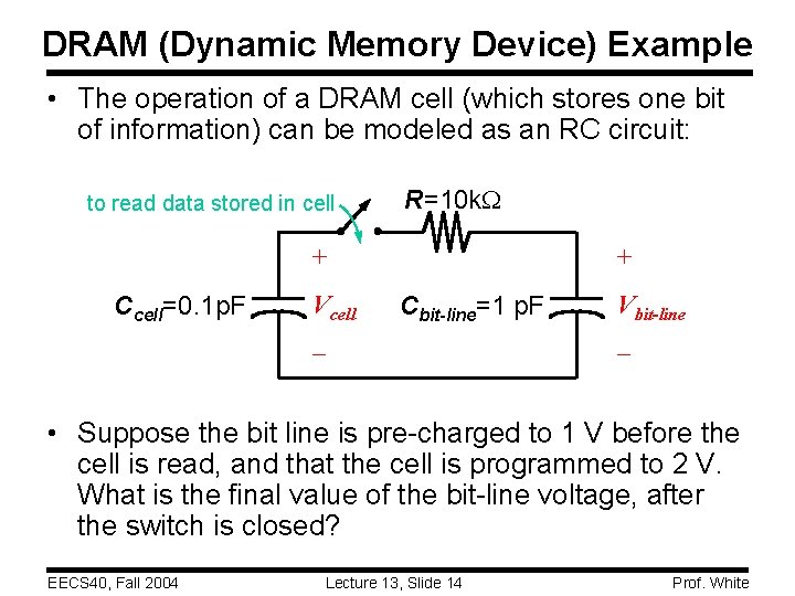
DRAM (Dynamic Memory Device) Example • The operation of a DRAM cell (which stores one bit of information) can be modeled as an RC circuit: to read data stored in cell R=10 k. W + Ccell=0. 1 p. F Vcell + Cbit-line=1 p. F – Vbit-line – • Suppose the bit line is pre-charged to 1 V before the cell is read, and that the cell is programmed to 2 V. What is the final value of the bit-line voltage, after the switch is closed? EECS 40, Fall 2004 Lecture 13, Slide 14 Prof. White
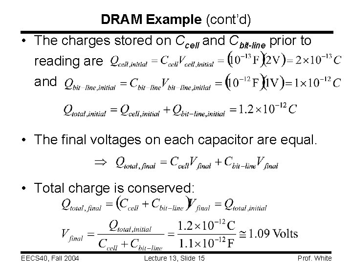
DRAM Example (cont’d) • The charges stored on Ccell and Cbit-line prior to reading are and • The final voltages on each capacitor are equal. • Total charge is conserved: EECS 40, Fall 2004 Lecture 13, Slide 15 Prof. White
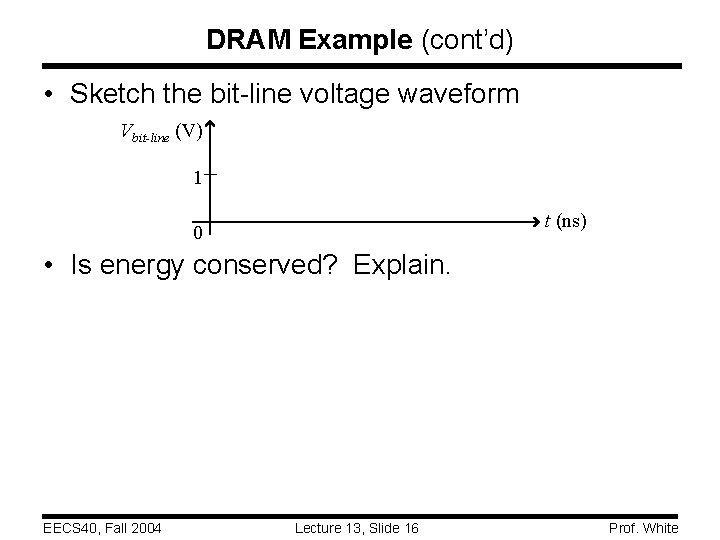
DRAM Example (cont’d) • Sketch the bit-line voltage waveform Vbit-line (V) 1 t (ns) 0 • Is energy conserved? Explain. EECS 40, Fall 2004 Lecture 13, Slide 16 Prof. White
Plan • We will be studying semiconductor devices and technology for the next several weeks – How does a transistor work? (need to learn about semiconductors and diode devices first) – How are transistors used as amplifiers? • modeled as dependent current source – How are transistors used to implement digital logic gates? • modeled as resistive switch (circuit performance is limited by RC delay) EECS 40, Fall 2004 Lecture 13, Slide 17 Prof. White