Inner Tracking Detector Upgrade Irradiation and Long Term

- Slides: 13

Inner Tracking Detector Upgrade Irradiation and Long Term Annealing: Issues and Comparisons Silas K Grossberndt March 2018 Update

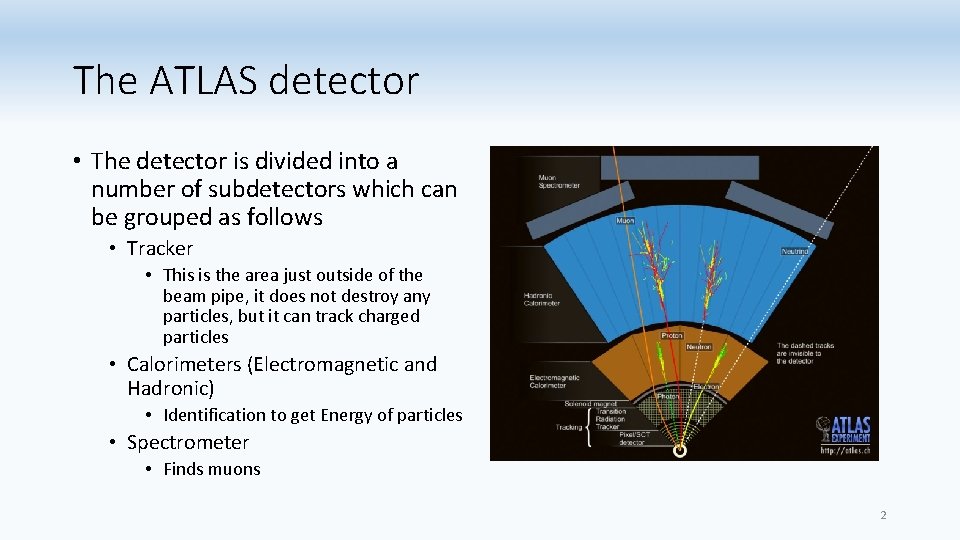
The ATLAS detector • The detector is divided into a number of subdetectors which can be grouped as follows • Tracker • This is the area just outside of the beam pipe, it does not destroy any particles, but it can track charged particles • Calorimeters (Electromagnetic and Hadronic) • Identification to get Energy of particles • Spectrometer • Finds muons 2

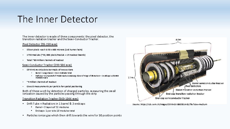
The Inner Detector The Inner detector is made of three components: the pixel detector, the transition radiation tracker and the Semi-Conductor Tracker. Pixel Detector (55 -150 mm) • Silicon pixels –each is 50 x 400 microns (1 x 8 human hairs) • 1750 modules (~50, 000 pixels/module + 16 readout boards) • Total: ~80 million channels of readout Semi-Conductor Tracker (299 -506 mm) • Si. PM micro-strip detector made of two sections • • Barrel—Long staves— 2112 modules total End Cap—Composed of Petals each containing slices of Rings of detectors— 2 endcaps with 988 modules each • ~6 million channels of readout • Gives 8 measurements per particle for spatial positioning Both of these work by detection of charged particles, measuring the small ionization caused by the particles passing through the strip Transition Radiation Tracker (563 -1066 mm) • Drift Tube + Radiatiors in 1 barrel & 2 endcaps • • Barrel— 3 layers of 32 modiules Endcaps- 1 per side 18 modules total • Particles ionize gas which then drift towards the wire for 30 position points Source: https: //cds. cern. ch/images/CERN-GE-0803014 -01/file? size=medium

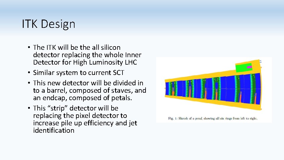
ITK Design • The ITK will be the all silicon detector replacing the whole Inner Detector for High Luminosity LHC • Similar system to current SCT • This new detector will be divided in to a barrel, composed of staves, and an endcap, composed of petals. • This “strip” detector will be replacing the pixel detector to increase pile up efficiency and jet identification

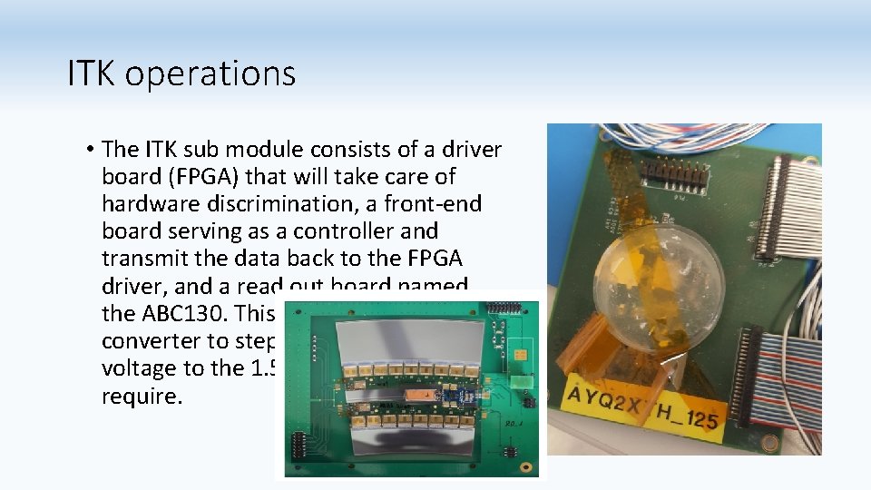
ITK operations • The ITK sub module consists of a driver board (FPGA) that will take care of hardware discrimination, a front-end board serving as a controller and transmit the data back to the FPGA driver, and a read out board named the ABC 130. This uses a DC-DC converter to step down supplied voltage to the 1. 5 V input that we require.

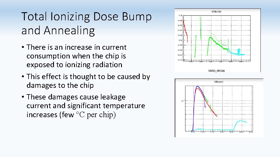
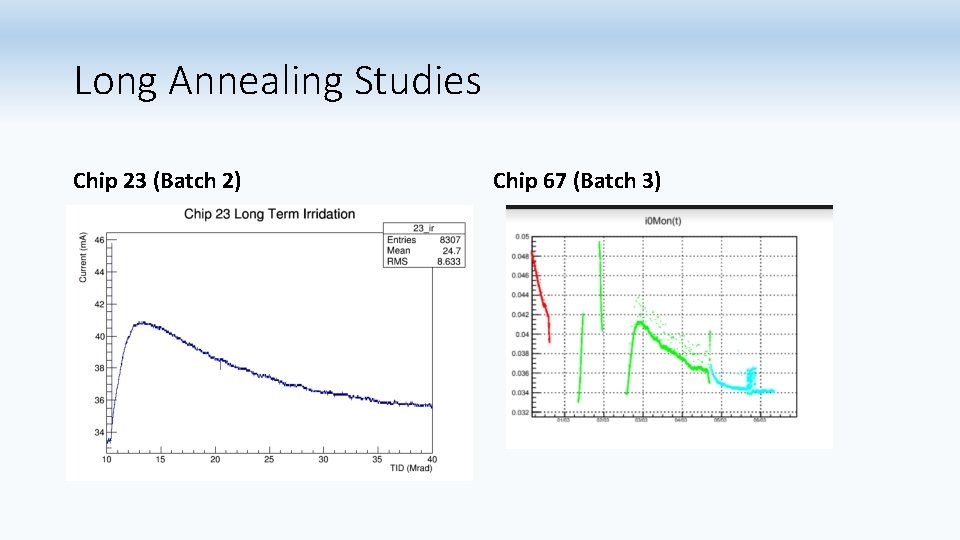
Total Ionizing Dose Bump and Annealing • There is an increase in current consumption when the chip is exposed to ionizing radiation • This effect is thought to be caused by damages to the chip • These damages cause leakage current and significant temperature increases (few °C per chip)

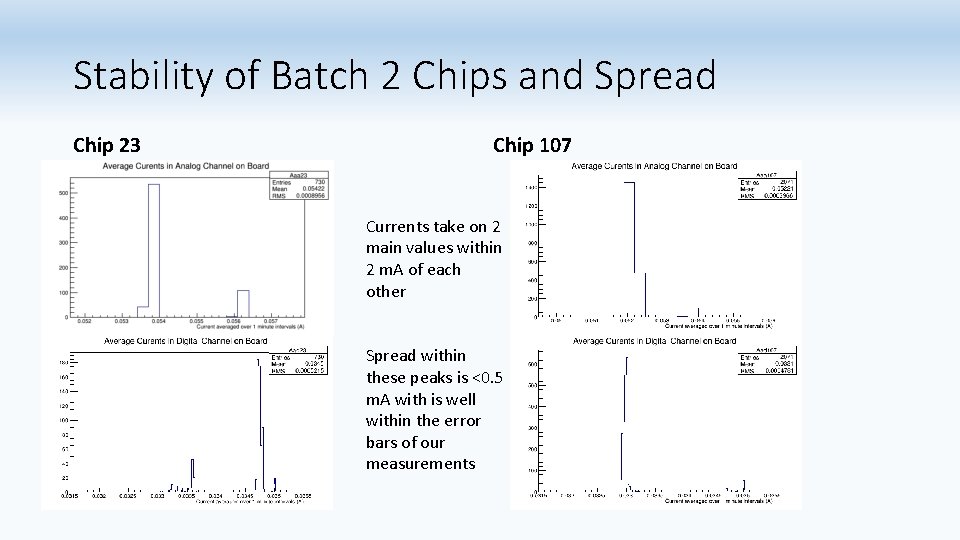
Stability of Batch 2 Chips and Spread Chip 23 Chip 107 Currents take on 2 main values within 2 m. A of each other Spread within these peaks is <0. 5 m. A with is well within the error bars of our measurements

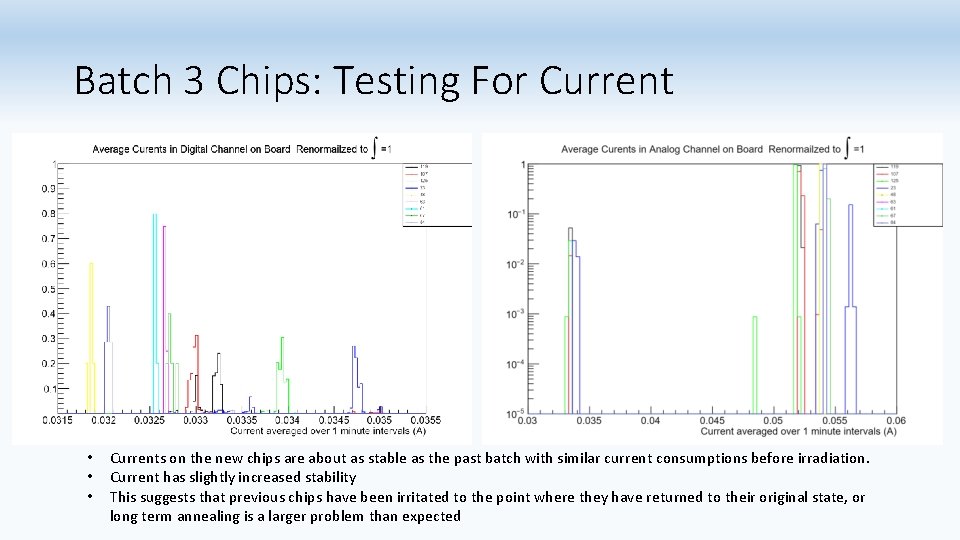
Batch 3 Chips: Testing For Current • • • Currents on the new chips are about as stable as the past batch with similar current consumptions before irradiation. Current has slightly increased stability This suggests that previous chips have been irritated to the point where they have returned to their original state, or long term annealing is a larger problem than expected

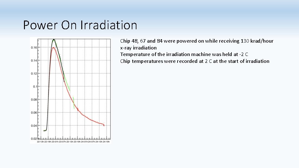
Power On Irradiation Chip 48, 67 and 84 were powered on while receiving 130 krad/hour x-ray irradiation Temperature of the irradiation machine was held at -2 C Chip temperatures were recorded at 2 C at the start of irradiation

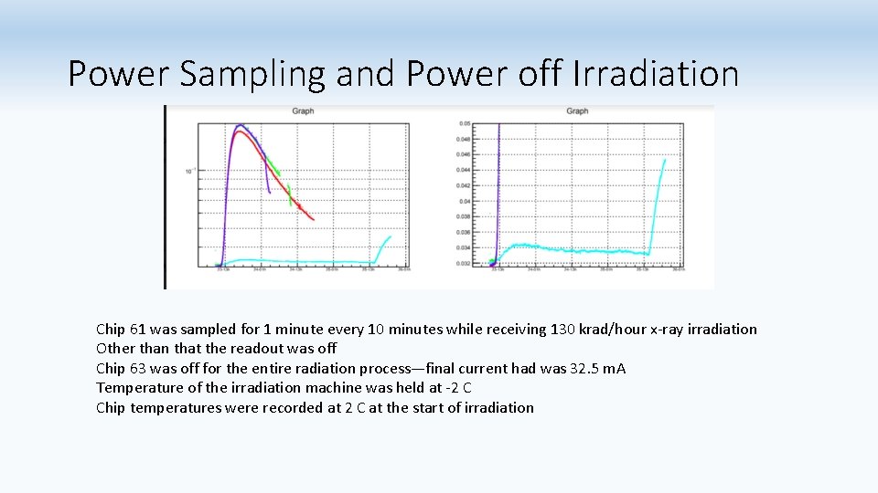
Power Sampling and Power off Irradiation Chip 61 was sampled for 1 minute every 10 minutes while receiving 130 krad/hour x-ray irradiation Other than that the readout was off Chip 63 was off for the entire radiation process—final current had was 32. 5 m. A Temperature of the irradiation machine was held at -2 C Chip temperatures were recorded at 2 C at the start of irradiation

Long Annealing Studies Chip 23 (Batch 2) Chip 67 (Batch 3)

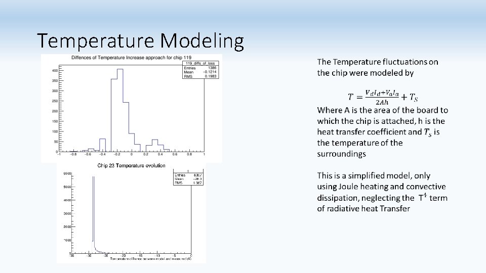
Temperature Modeling

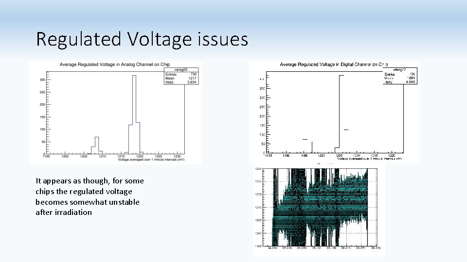
Regulated Voltage issues It appears as though, for some chips the regulated voltage becomes somewhat unstable after irradiation