Firmware Overview and Status Erno DAVID Wigner Research
- Slides: 10
Firmware Overview and Status Erno DAVID Wigner Research Center for Physics (HU) 26 January, 2016
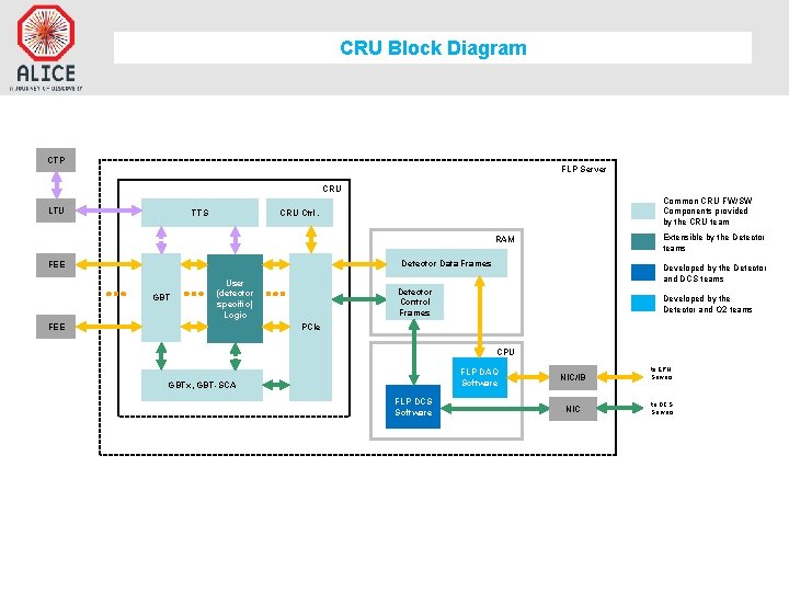
CRU Block Diagram CTP FLP Server CRU LTU TTS Common CRU FW/SW Components provided by the CRU team CRU Ctrl. Extensible by the Detector teams RAM Detector Data Frames FEE GBT User (detector specific) Logic FEE Developed by the Detector and DCS teams Detector Control Frames Developed by the Detector and O 2 teams PCIe CPU FLP DAQ Software GBTx, GBT-SCA FLP DCS Software NIC/IB to EPN Servers NIC to DCS Servers
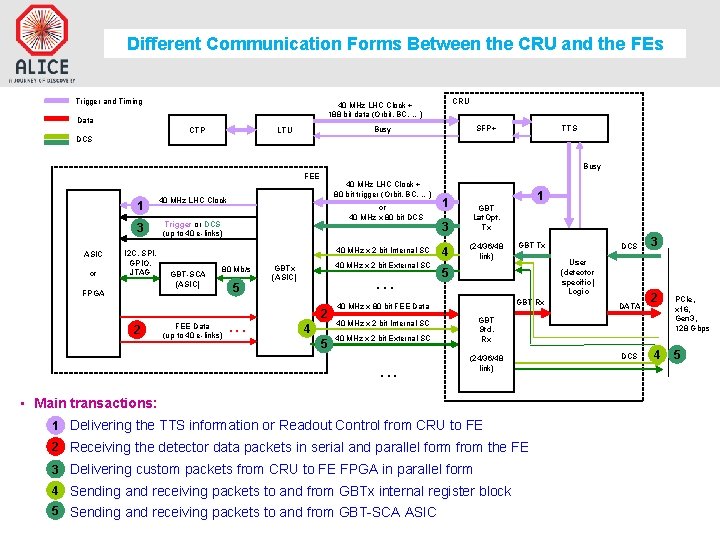
Different Communication Forms Between the CRU and the FEs Trigger and Timing CRU 40 MHz LHC Clock + 188 bit data (Orbit, BC, …) Data SFP+ Busy LTU CTP TTS DCS Busy FEE ASIC or 1 40 MHz LHC Clock . 3. . Trigger or DCS (up to 40 e-links) I 2 C, SPI, GPIO, JTAG FPGA 40 MHz LHC Clock + 80 bit trigger (Orbit, BC, …) or 40 MHz x 80 bit DCS 40 MHz x 2 bit Internal SC GBT-SCA (ASIC) 80 Mb/s 5 40 MHz x 2 bit External SC GBTx (ASIC) . . . 2. . FEE Data (up to 40 e-links) . . . 4 5 1 1 3 GBT Lat. Opt. Tx 4 (24/36/48 link) GBT Rx DATA 3 2 GBT Std. Rx 40 MHz x 2 bit Internal SC 40 MHz x 2 bit External SC (24/36/48 link) • Main transactions: 1 • Delivering the TTS information or Readout Control from CRU to FE 2 • Receiving the detector data packets in serial and parallel form from the FE 3 • Delivering custom packets from CRU to FE FPGA in parallel form 4 • Sending and receiving packets to and from GBTx internal register block 5 • Sending and receiving packets to and from GBT-SCA ASIC DCS User (detector specific) Logic 5 40 MHz x 80 bit FEE Data . . . GBT Tx DCS 4 PCIe, x 16, Gen 3, 128 Gbps 5
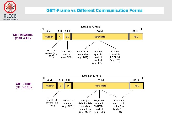
GBT-Frame vs Different Communication Forms 120 bit @ 40 MHz GBT Downlink (CRU -> FE) 4 bit 2 bit 80 bit 32 bit Header IC EC User Data FEC GBTx reg. access (e. g. TPC) GBT-SCA comm. (e. g. TPC) 80 bit TTS information (e. g. TOF) Detector specific readout control (e. g. TPC) Custom packet for FE FPGA (e. g. ITS) 120 bit @ 40 MHz GBT Uplink (FE -> CRU) 4 bit 2 bit 80 bit 32 bit Header IC EC User Data FEC GBTx reg. access (e. g. TPC) GBT-SCA comm. (e. g. TPC) Multiple Single well detector data formed packets in CDH/SDH serial form packet (e. g. MCH) (e. g. TOF) Raw frontend data in Wide Bus Mode (e. g. TPC)
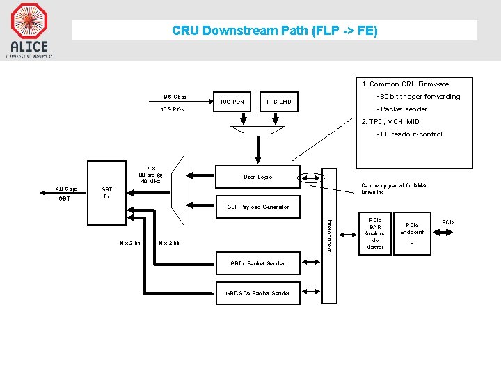
CRU Downstream Path (FLP -> FE) 1. Common CRU Firmware 9. 6 Gbps 10 G PON • 80 bit trigger forwarding TTS EMU • Packet sender 10 G PON 2. TPC, MCH, MID • FE readout-control Nx 80 bits @ 40 MHz 4. 8 Gbps GBT User Logic Can be upgraded for DMA Downlink GBT Tx GBT Payload Generator Interconnect N x 2 bit GBTx Packet Sender GBT-SCA Packet Sender PCIe BAR Avalon. MM Master PCIe Endpoint 0 PCIe
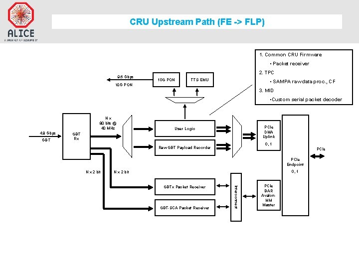
CRU Upstream Path (FE -> FLP) 1. Common CRU Firmware • Packet receiver 9. 6 Gbps 2. TPC 10 G PON TTS EMU • SAMPA raw data proc. , CF 10 G PON 3. MID • Custom serial packet decoder Nx 80 bits @ 40 MHz 4. 8 Gbps GBT PCIe DMA Uplink User Logic GBT Rx 0, 1 Raw GBT Payload Recorder PCIe Endpoint N x 2 bit 0, 1 N x 2 bit GBT-SCA Packet Receiver Interconnect GBTx Packet Receiver PCIe BAR Avalon. MM Master
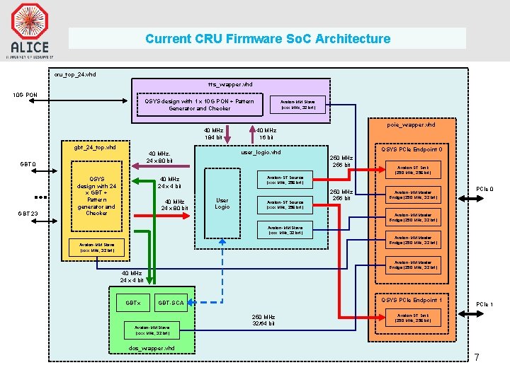
Current CRU Firmware So. C Architecture cru_top_24. vhd tts_wrapper. vhd 10 G PON QSYS design with 1 x 10 G PON + Pattern Generator and Checker 40 MHz 184 bit gbt_24_top. vhd GBT 23 40 MHz 24 x 80 bit QSYS PCIe Endpoint 0 250 MHz 256 bit Avalon-ST Sink (250 MHz, 256 bit) Avalon-ST Source (xxx MHz, 256 bit) 40 MHz 24 x 4 bit QSYS design with 24 x GBT + Pattern generator and Checker pcie_wrapper. vhd 40 MHz 16 bit user_logic. vhd 40 MHz, 24 x 80 bit GBT 0 Avalon-MM Slave (xxx MHz, 32 bit) User Logic Avalon-ST Source (xxx MHz, 256 bit) 250 MHz 256 bit Avalon-MM Master Bridge (250 MHz, 32 bit) PCIe 0 Avalon-MM Master Bridge (250 MHz, 32 bit) Avalon-MM Slave (xxx MHz, 32 bit) Avalon-MM Master Bridge (250 MHz, 32 bit) 40 MHz 24 x 4 bit GBTx QSYS PCIe Endpoint 1 GBT-SCA Avalon-MM Slave (xxx MHz, 32 bit) 250 MHz 32/64 bit PCIe 1 Avalon-ST Sink (250 MHz, 256 bit) dcs_wrapper. vhd 7
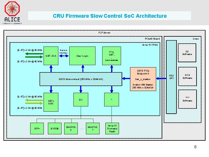
CRU Firmware Slow Control So. C Architecture FLP Server PCIe 40 Board Linux Arria 10 FPGA [0. . 47] x 2 bit @ 40 MHz Custom Interface GBT-SCA User Logic O 2 Software TTS, GBT, … (core modules) [0. . 47] x 2 bit @ 40 MHz QSYS PCIe Endpoint 0 bar_x_master QSYS Interconnect (250 MHz x 32/64 bit) CRU API DCS Software Avalon-MM Master 250 MHz x 32/64 bit [0. . 47] x 2 bit @ 40 MHz I 2 C GBTx ASIC ? ? ? ? Software [0. . 47] x 2 bit @ 40 MHz SFP+ Si 5338 Mini. POD 0 . . . Mini. POD 7 Arria 10 Firmware Flash 8
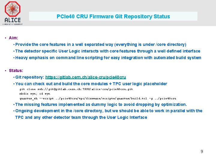
PCIe 40 CRU Firmware Git Repository Status • Aim: • Provide the core features in a well separated way (everything is under /core directory) • The detector specific User Logic interacts with core features through a well defined interface • Heavy emphasis on command line scripting for easy integration with automated build system • Status: • Git repository: https: //gitlab. cern. ch/alice-cru/pcie 40 cru • You can check out and build the core modules + TPC user logic placeholder git clone ssh: //git@gitlab. cern. ch: 7999/alice-cru/pcie 40 cru. git mkdir syn; cd syn quartus_sh --script. . /pcie 40 cru/tpc/firmware/scripts/quartus/build. tcl -g. . /pcie 40 cru • The missing features implemented as dummy logic to avoid dropping by optimization. • Ongoing development in the /core directory, but we should be able to work in parallel with the TPC and any other detector team through the User Logic Interface 9
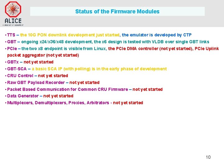
Status of the Firmware Modules • TTS – the 10 G PON downlink development just started, the emulator is developed by CTP • GBT – ongoing x 24/x 36/x 48 development, the x 6 design is tested with VLDB over single GBT links • PCIe – the two x 8 endpoint is visible from Linux, the PCIe DMA controller (not yet started), PCIe Uplink packet aggregator (not yet started) • GBTx – not yet started • GBT-SCA – a basic SCA IP (with polling) is in the early phase of development • CRU Control – not yet started • Raw GBT Payload Recorder – not yet started • Packet Based Communication for Common CRU Firmware – not yet started • Data Generator – not yet started • Multiplexers, Demultiplexers, Proxies, Arbitrators - not yet started 10