ENGR ECE 212 11 14 April 2003 All

- Slides: 19

ENGR / ECE 212 11 & 14 April, 2003 All slides except those with blue backgrounds are taken from John Wakerly’s Stanford EE 121, Digital Design Laboratory 1

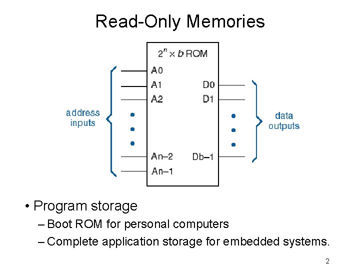
Read-Only Memories • Program storage – Boot ROM for personal computers – Complete application storage for embedded systems. 2

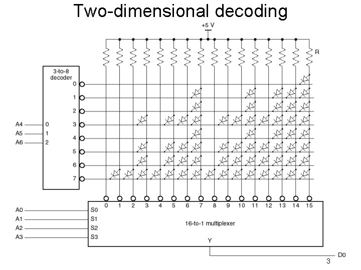
Two-dimensional decoding 3

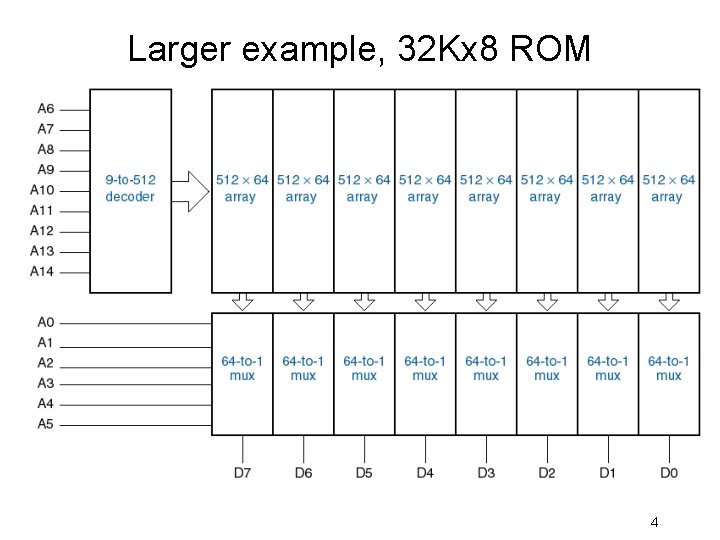
Larger example, 32 Kx 8 ROM 4

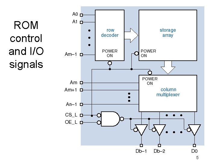
ROM control and I/O signals 5

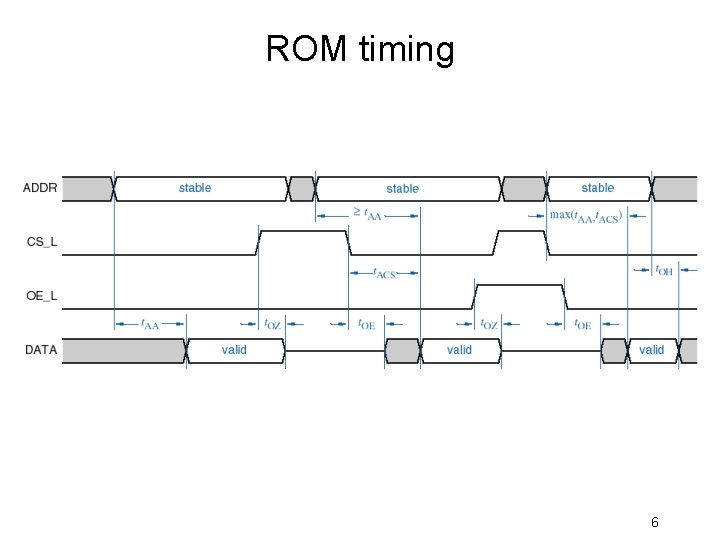
ROM timing 6

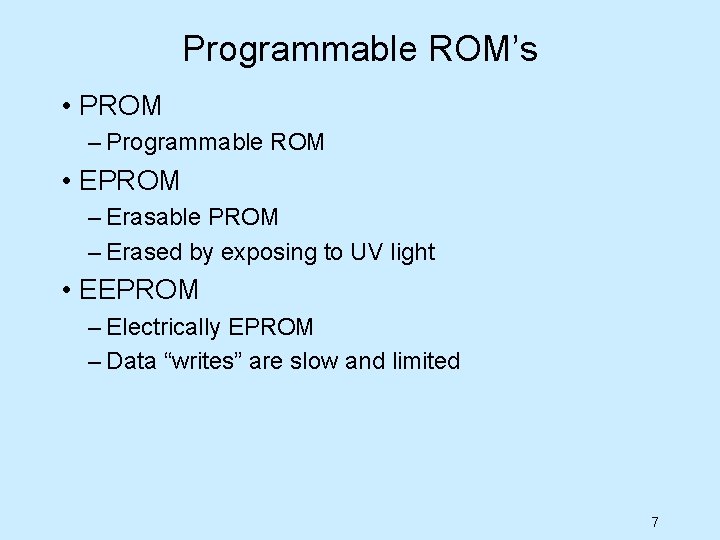
Programmable ROM’s • PROM – Programmable ROM • EPROM – Erasable PROM – Erased by exposing to UV light • EEPROM – Electrically EPROM – Data “writes” are slow and limited 7

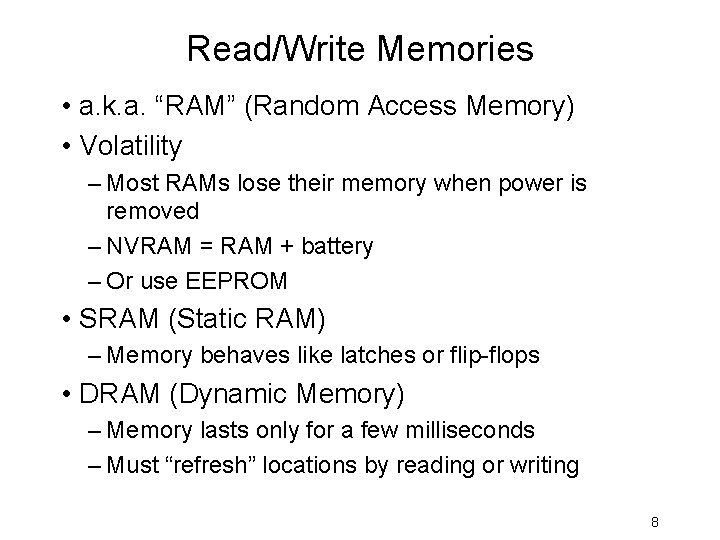
Read/Write Memories • a. k. a. “RAM” (Random Access Memory) • Volatility – Most RAMs lose their memory when power is removed – NVRAM = RAM + battery – Or use EEPROM • SRAM (Static RAM) – Memory behaves like latches or flip-flops • DRAM (Dynamic Memory) – Memory lasts only for a few milliseconds – Must “refresh” locations by reading or writing 8

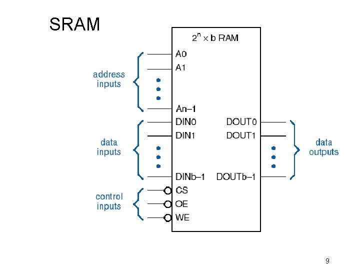
SRAM 9

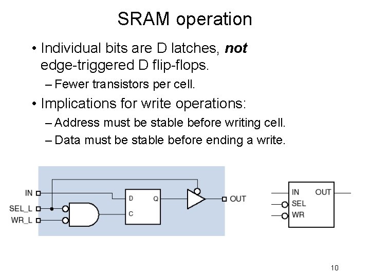
SRAM operation • Individual bits are D latches, not edge-triggered D flip-flops. – Fewer transistors per cell. • Implications for write operations: – Address must be stable before writing cell. – Data must be stable before ending a write. 10

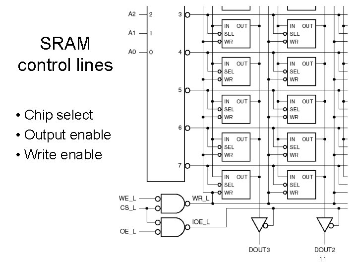
SRAM control lines • Chip select • Output enable • Write enable 11

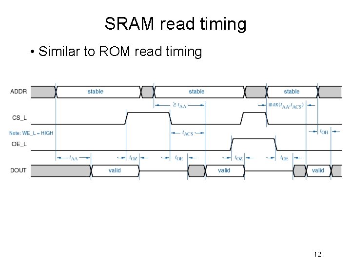
SRAM read timing • Similar to ROM read timing 12

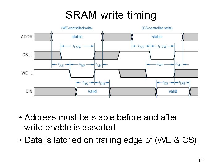
SRAM write timing • Address must be stable before and after write-enable is asserted. • Data is latched on trailing edge of (WE & CS). 13

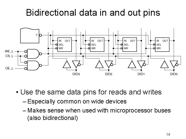
Bidirectional data in and out pins • Use the same data pins for reads and writes – Especially common on wide devices – Makes sense when used with microprocessor buses (also bidirectional) 14

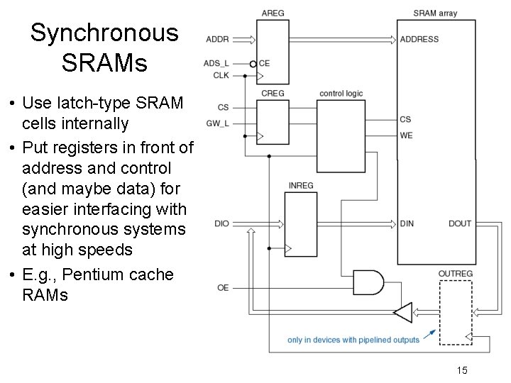
Synchronous SRAMs • Use latch-type SRAM cells internally • Put registers in front of address and control (and maybe data) for easier interfacing with synchronous systems at high speeds • E. g. , Pentium cache RAMs 15

Some real life examples 64 -bit (16 4) RAM Intel’s specification for 133 Mhz SDRAM IBM SRAM 64 k bit EEPROM 16

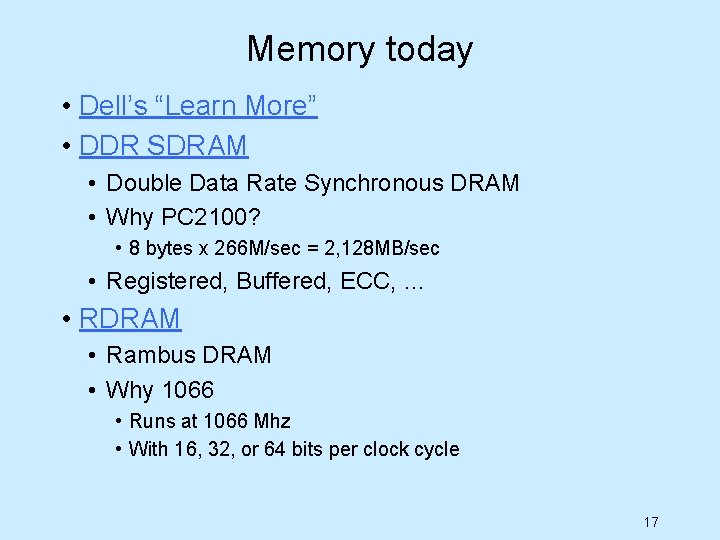
Memory today • Dell’s “Learn More” • DDR SDRAM • Double Data Rate Synchronous DRAM • Why PC 2100? • 8 bytes x 266 M/sec = 2, 128 MB/sec • Registered, Buffered, ECC, … • RDRAM • Rambus DRAM • Why 1066 • Runs at 1066 Mhz • With 16, 32, or 64 bits per clock cycle 17

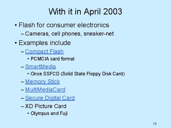
With it in April 2003 • Flash for consumer electronics – Cameras, cell phones, sneaker-net • Examples include – Compact Flash • PCMCIA card format – Smart. Media • Once SSFCD (Solid State Floppy Disk Card) – Memory Stick – Multi. Media. Card – Secure Digital Card – XD Picture Card • Olympus and Fuji 18

How Stuff Works • ROM • RAM • Flash memory • Computer memory 19