DHH progress report Igor Konorov TUM Physics Department
- Slides: 11

DHH progress report Igor Konorov TUM, Physics Department, E 18 DEPFET workshop, Bonn February 7 -9, 2011 Outline: q Implementation synchronous clock distribution using Xilinx V 5 GTP q Summary and outlook

Why Xilinx FPGA Motivation to use Xilinx FPGA instead of Lattice FPGA – Belle II RO electronics and ATCA based on Xilinx FPGAs – New IHEP ATCA design utilizes SFP+ and FPGAs capable to run up to 6 Gbps – KEK colleagues study Xilinx FPGA SEU in neutron irradiation – Xilinx FPGAs radiation tolerance should be higher due to partial reconfiguration capability DEPFET workshop, Bonn И. Коноров, TUM 2

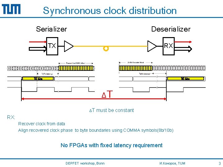
Synchronous clock distribution Serializer Deserializer TX RX 16 bits ΔT ΔT must be constant RX: Recover clock from data Align recovered clock phase to byte boundaries using COMMA symbols(8 b/10 b) No FPGAs with fixed latency requirement DEPFET workshop, Bonn И. Коноров, TUM 3

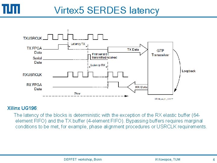
Virtex 5 SERDES latency Xilinx UG 196: The latency of the blocks is deterministic with the exception of the RX elastic buffer (64 element FIFO) and the TX buffer (4 -element FIFO). Bypassing buffers requires marginal conditions to be met, for example, phase alignment procedures or USRCLK requirements. DEPFET workshop, Bonn И. Коноров, TUM 4

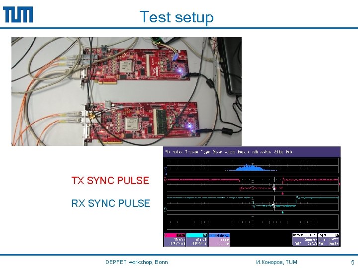
Test setup TX SYNC PULSE RX SYNC PULSE DEPFET workshop, Bonn И. Коноров, TUM 5

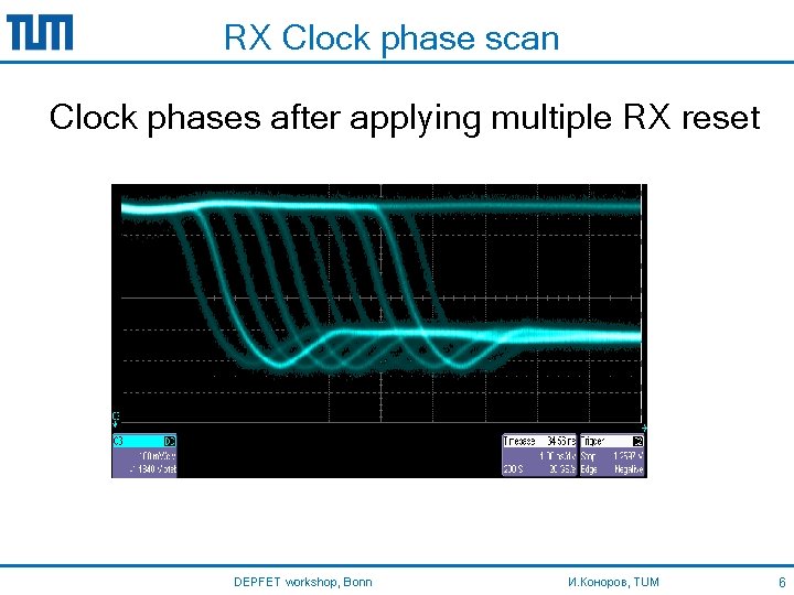
RX Clock phase scan Clock phases after applying multiple RX reset DEPFET workshop, Bonn И. Коноров, TUM 6

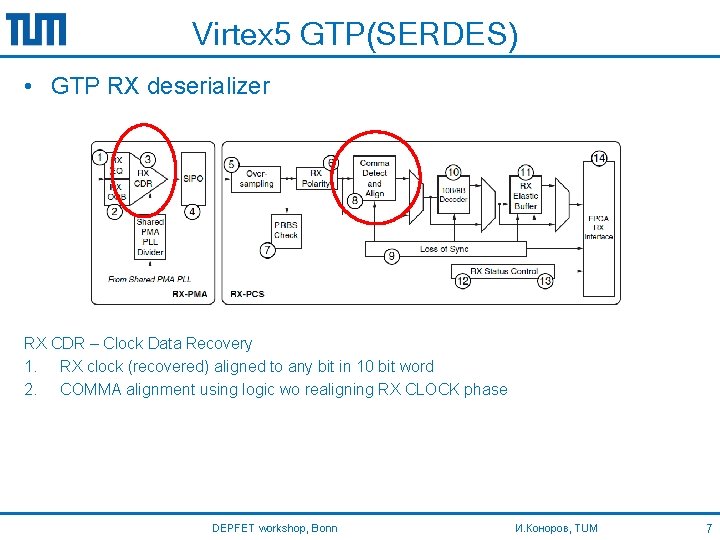
Virtex 5 GTP(SERDES) • GTP RX deserializer RX CDR – Clock Data Recovery 1. RX clock (recovered) aligned to any bit in 10 bit word 2. COMMA alignment using logic wo realigning RX CLOCK phase DEPFET workshop, Bonn И. Коноров, TUM 7

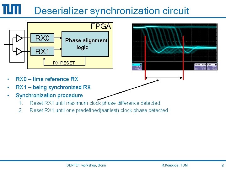
Deserializer synchronization circuit FPGA RX 0 RX 1 Phase alignment logic RX RESET • • • RX 0 – time reference RX RX 1 – being synchronized RX Synchronization procedure 1. 2. Reset RX 1 until maximum clock phase difference detected Reset RX 1 until one predefined(earliest) clock phase detected DEPFET workshop, Bonn И. Коноров, TUM 8

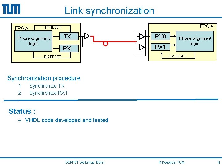
Link synchronization FPGA TX RESET FPGA Phase alignment logic TX RX 0 RX RX 1 Phase alignment logic RX RESET Synchronization procedure 1. 2. Synchronize TX Synchronize RX 1 Status : – VHDL code developed and tested DEPFET workshop, Bonn И. Коноров, TUM 9

Summary • Virtex 5 GTP features evaluated and allow to implement synchronous link • VHDL code for synchronous link implementation complete • Long term test to be done DEPFET workshop, Bonn И. Коноров, TUM 10

Outlook • Questions: – DHP DHH cable interface – Slow control and online data processing • • Reading full frame Pedestal calculation Pedestal loading via JTAG Reading full frame via JTAG an option? • DHH system design to be finalized later • Next steps (mostly VHDL code development using ev. cards) – DHH ATCA - discussion with Soeren and Zhen’an – DHP DHH – discussion with Hans – DHH module schematic DEPFET workshop, Bonn И. Коноров, TUM 11