Design of a telescopic fullydifferential OTA Aseem Sayal

- Slides: 17

Design of a telescopic fully-differential OTA Aseem Sayal, Vipul Goyal Graduate Student, Electrical and Computer Engg. The University of Texas at Austin

Contents • Executive Summary • Circuit Design • Design Methodology and Tradeoffs • Simulation Results • Performance Evaluation • Design Efforts and Learnings • Conclusion • References

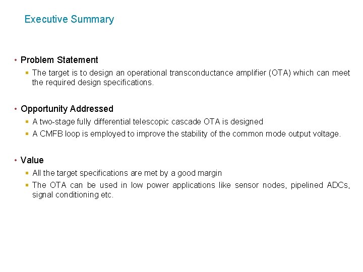
Executive Summary • Problem Statement § The target is to design an operational transconductance amplifier (OTA) which can meet the required design specifications. • Opportunity Addressed § A two-stage fully differential telescopic cascade OTA is designed § A CMFB loop is employed to improve the stability of the common mode output voltage. • Value § All the target specifications are met by a good margin § The OTA can be used in low power applications like sensor nodes, pipelined ADCs, signal conditioning etc.

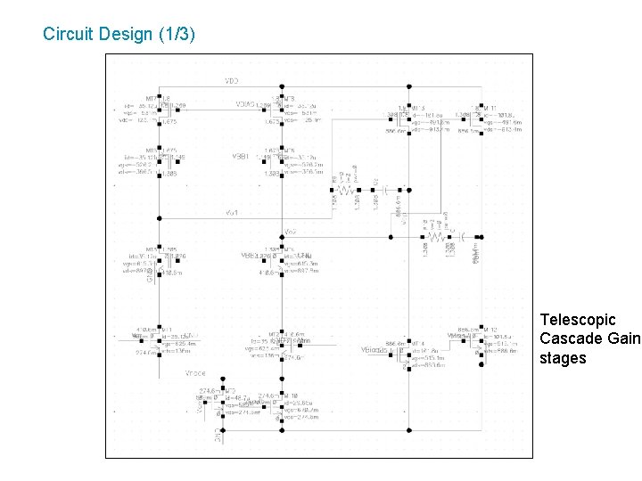
Circuit Design (1/3) Telescopic Cascade Gain stages

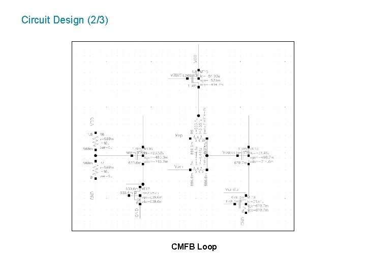
Circuit Design (2/3) CMFB Loop

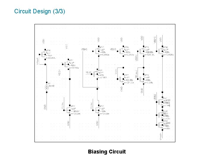
Circuit Design (3/3) Biasing Circuit

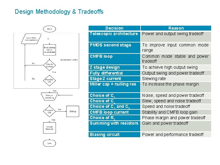
Design Methodology & Tradeoffs Decision Telescopic architecture Reason Power and output swing tradeoff PMOS second stage 2 stage design Fully differential Stage 2 current Miller cap + nulling res To improve input common mode range Common mode stable and power tradeoff To achieve high output swing Output swing and power tradeoff Slewing rate To increase the phase margin Choice of Cc Choice of CL Choice of C 1 and C 2 CMFB loop current Choice of RZ Summing with resistors Noise, speed and power tradeoff Slew, speed and noise tradeoff Stability and CMFB loop gain Phase margin and power tradeoff Gain and power tradeoff Biasing circuit Power and performance tradeoff CMFB loop

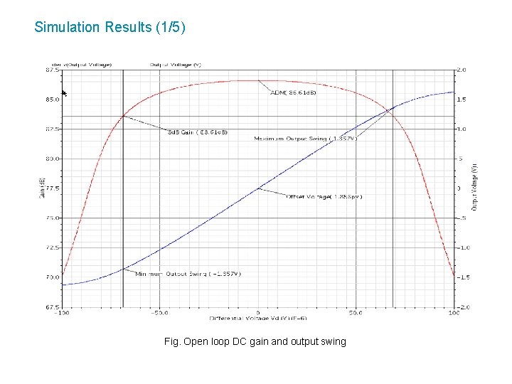
Simulation Results (1/5) Fig. Open loop DC gain and output swing

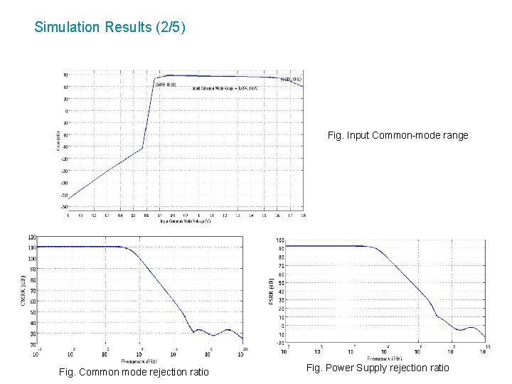
Simulation Results (2/5) Fig. Input Common-mode range Fig. Common mode rejection ratio Fig. Power Supply rejection ratio

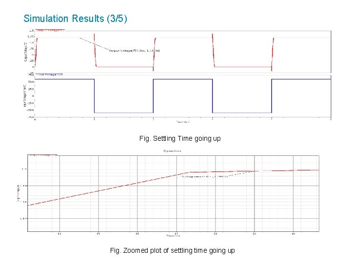
Simulation Results (3/5) Fig. Settling Time going up Fig. Zoomed plot of settling time going up

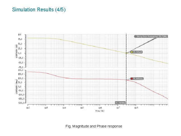
Simulation Results (4/5) Fig. Magnitude and Phase response

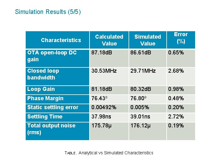
Simulation Results (5/5) Characteristics Calculated Value Simulated Value Error (%) OTA open-loop DC gain 87. 18 d. B 86. 61 d. B 0. 65% Closed loop bandwidth 30. 53 MHz 29. 71 MHz 2. 68% Loop Gain 81. 18 d. B 80. 32 d. B 0. 98% Phase Margin 76. 43 o 76. 80 o 0. 48% Static settling error 0. 00492% 0. 005% 0. 20% Settling Time 37. 98 ns 39. 01 ns 2. 72% Total output noise (rms) 175. 78µ 176. 12µ 0. 19% TABLE. Analytical vs Simulated Characteristics

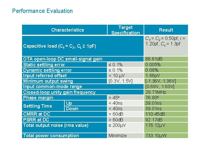
Performance Evaluation Characteristics Target Specification Result Capacitive load (C 1 = C 2, CL ≥ 1 p. F) C 1 = C 2 = 0. 50 pf, i = 1. 20 pf, Cc = 1. 3 pf OTA open-loop DC small-signal gain Static settling error Dynamic settling error Input referred offset Minimum output swing Input common-mode range Closed-loop unity gain frequency Phase margin Up Settling Time Down CMRR at DC PSRR at DC Total output noise (rms value) > 45 o < 40 ns > 60 d. B ≤ 200µV 86. 61 d. B 0. 005% 0. 08% 1. 86 p. V [-1. 36 V, 1. 36 V] [0. 69 V, 1. 63 V] 29. 71 MHz 76. 80 o 39. 01 ns 110. 45 d. B 92. 17 d. B 176. 12µV Minimize 733. 10µW Total power consumption ≤ 0. 1% < 10 µV [0. 3 V, 1. 5 V]

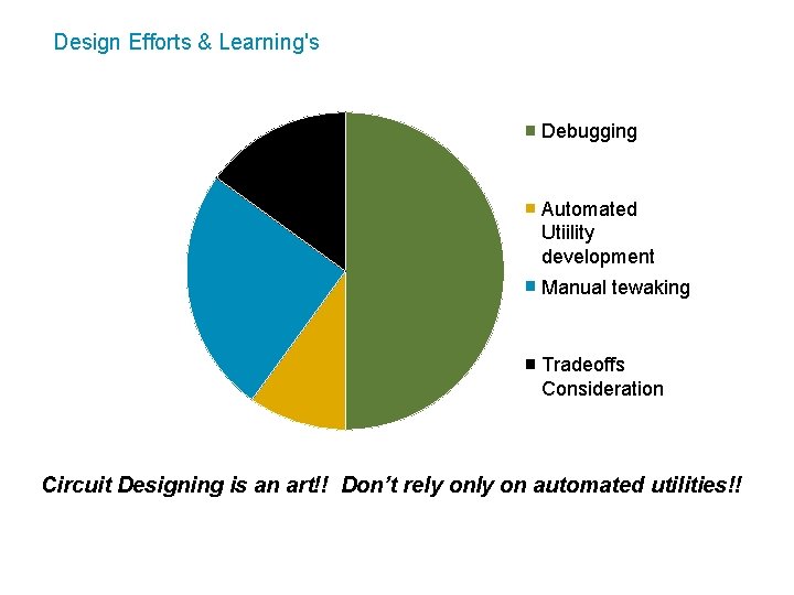
Design Efforts & Learning's Debugging Automated Utiility development Manual tewaking Tradeoffs Consideration Circuit Designing is an art!! Don’t rely on automated utilities!!

Conclusion • A low power fully differential telescopic operational Transconductance amplifier employing CMFB loop is designed to meet the required specifications. • The comprehensive circuit design analysis is performed and design methodology is presented. • The simulation results are included to verify the correctness of the design and to quantify the error with the calculated values. • The performance evaluation is performed to prove that the target specifications are met by a good margin. • Thus, this circuit can be used in various applications such as sensor nodes, pipelined ADCs, signal conditioning etc.

References • Liu M, Huang K, Ou W, et al. A low power 13 -bit 16 MSPS CMOS pipeline ADC. IEEE J Solid-State Circuits, 2004. • Ming B, Kim P, Bowman F W, et al. A 69 m. W 10 -bit 80 MSample/s pipeline ADC. IEEE J Solid-State Circuits, 2003. • Paul Gray et al. , Analysis and Design of Analog Integrated Circuits, Wiley, 2009. • Behzad Razavi, Design of Analog CMOS Integrated Circuits, Mc. Graw-Hill, 2000. • Yao Zhijian, Ma Chengyan, Ye Tianchan, et al. Design and analysis of a gain-enhanced fully differential telescopic operational transconductance amplifier. Journal of Semiconductors, 2008. • Gulati K, Lee H S. A high swing telescopic operational ampli- fier. IEEE J Solid-State Circuits, 1998, 33(12): 2010. • Rezaei M, Zhian-Tabasy E, Ashtiani S J. Slew rate enhancement method for folded-cascode amplifier. Electron Lett, 2008. • Phillip Allen et al, CMOS Analog Circuit Design, Oxford University Press, 2002. • David Johns and Ken Martin, Analog Integrated Circuit Design, Wiley, 1996.

QA