Charge Multiplication Properties in Highly Irradiated Thin Epitaxial
- Slides: 16

Charge Multiplication Properties in Highly Irradiated Thin Epitaxial Silicon Diodes Jörn Lange, Julian Becker, Eckhart Fretwurst, Robert Klanner, Gunnar Lindström Hamburg University 15 th RD 50 Workshop, CERN, November 2009 In the framework of the CERN RD 50 Collaboration

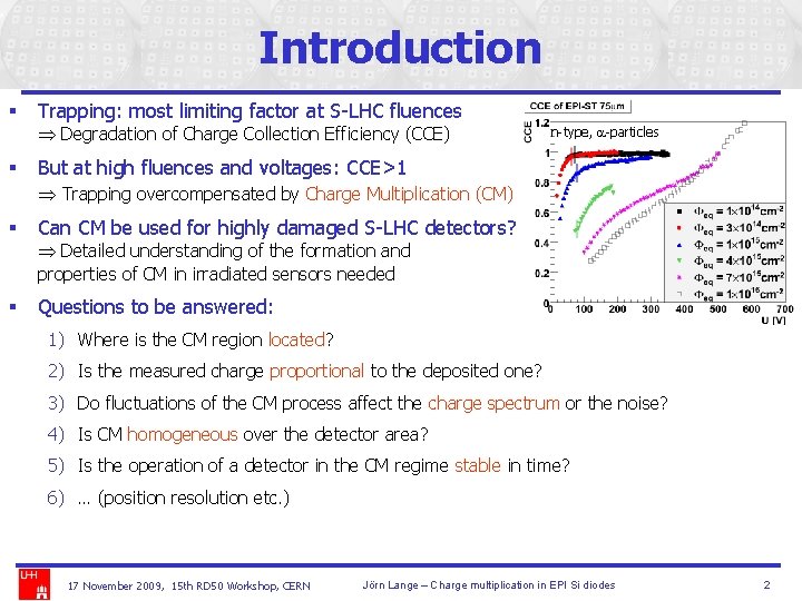
Introduction § Trapping: most limiting factor at S-LHC fluences Degradation of Charge Collection Efficiency (CCE) § n-type, a-particles But at high fluences and voltages: CCE>1 Trapping overcompensated by Charge Multiplication (CM) § Can CM be used for highly damaged S-LHC detectors? Detailed understanding of the formation and properties of CM in irradiated sensors needed § Questions to be answered: 1) Where is the CM region located? 2) Is the measured charge proportional to the deposited one? 3) Do fluctuations of the CM process affect the charge spectrum or the noise? 4) Is CM homogeneous over the detector area? 5) Is the operation of a detector in the CM regime stable in time? 6) … (position resolution etc. ) 17 November 2009, 15 th RD 50 Workshop, CERN Jörn Lange – Charge multiplication in EPI Si diodes 2

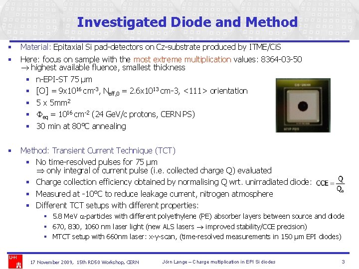
Investigated Diode and Method § § Material: Epitaxial Si pad-detectors on Cz-substrate produced by ITME/Ci. S § Method: Transient Current Technique (TCT) § No time-resolved pulses for 75 µm only integral of current pulse (i. e. collected charge Q) evaluated § Charge collection efficiency obtained by normalising Q wrt. unirradiated diode: § Measured at -10°C to reduce leakage current, nitrogen atmosphere § Different TCT setups with different properties: Here: focus on sample with the most extreme multiplication values: 8364 -03 -50 highest available fluence, smallest thickness § n-EPI-ST 75 µm § [O] = 9 x 1016 cm-3, Neff, 0 = 2. 6 x 1013 cm-3, <111> orientation § 5 x 5 mm 2 § Feq = 1016 cm-2 (24 Ge. V/c protons, CERN PS) § 30 min at 80°C annealing § 5. 8 Me. V a-particles with different polyethylene (PE) absorber layers between source and diode § 670, 830, 1060 nm laser light (new ALS lasers improved stability/CCE precision) § MTCT setup with 660 nm laser: x-y-scan, (time-resolved measurements in 150 µm EPI diodes) 17 November 2009, 15 th RD 50 Workshop, CERN Jörn Lange – Charge multiplication in EPI Si diodes 3

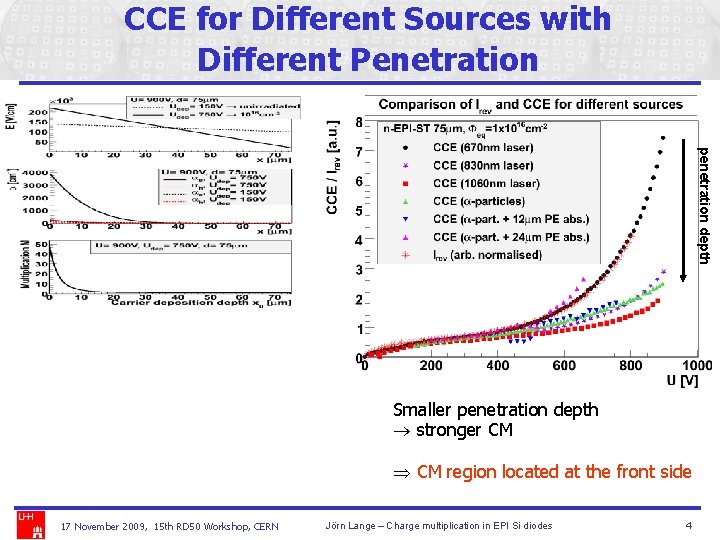
CCE for Different Sources with Different Penetration penetration depth Smaller penetration depth stronger CM region located at the front side 17 November 2009, 15 th RD 50 Workshop, CERN Jörn Lange – Charge multiplication in EPI Si diodes 4

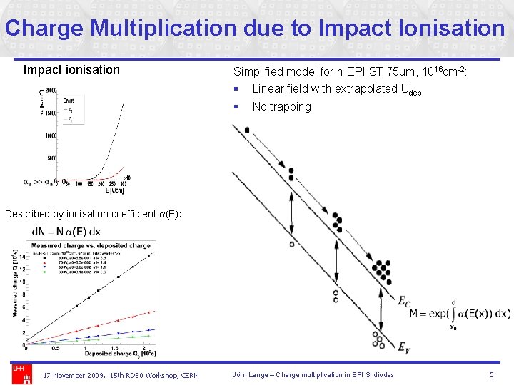
Charge Multiplication due to Impact Ionisation Impact ionisation Simplified model for n-EPI ST 75µm, 1016 cm-2: § § Linear field with extrapolated Udep No trapping Described by ionisation coefficient a(E): 17 November 2009, 15 th RD 50 Workshop, CERN Jörn Lange – Charge multiplication in EPI Si diodes 5

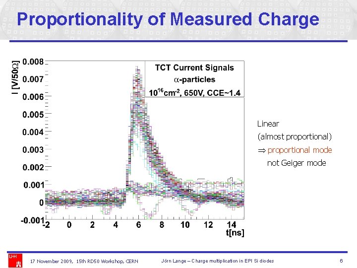
Proportionality of Measured Charge Linear (almost proportional) proportional mode not Geiger mode 17 November 2009, 15 th RD 50 Workshop, CERN Jörn Lange – Charge multiplication in EPI Si diodes 6

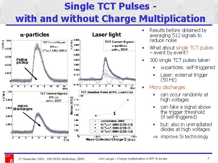
Single TCT Pulses with and without Charge Multiplication a-particles Peltier pickup Laser light § Results before obtained by averaging 512 signals to reduce noise § What about single TCT pulses – event by event? § 300 single TCT pulses taken § § § micro discharges a-particles: self-triggered Laser: external trigger (50 Hz) Micro discharges § can occur randomly at high voltages § can fake a signal above the trigger threshold (if self-triggered) § but: also in unirradiated diodes at high voltages improve Si technology 17 November 2009, 15 th RD 50 Workshop, CERN Jörn Lange – Charge multiplication in EPI Si diodes 7

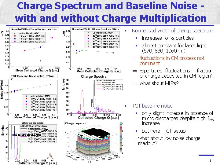
Charge Spectrum and Baseline Noise with and without Charge Multiplication § Normalised width of charge spectrum: § increases for a-particles § almost constant for laser light (670, 830, 1060 nm) fluctuations in CM process not dominant a-particles: fluctuations in fraction of charge deposited in CM region? what about MIPs? § incl. micro discharges 17 November 2009, 15 th RD 50 Workshop, CERN TCT baseline noise § only slight increase in absence of micro discharges despite high Irev increase § but here: TCT setup what about low noise charge readout? Jörn Lange – Charge multiplication in EPI Si diodes 8

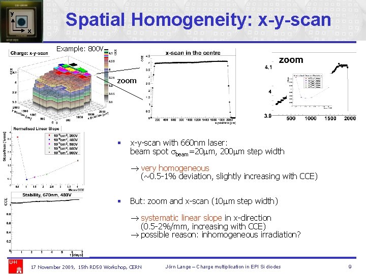
y x Spatial Homogeneity: x-y-scan Example: 800 V zoom § x-y-scan with 660 nm laser: beam spot sbeam=20 mm, 200 mm step width very homogeneous (~0. 5 -1% deviation, slightly increasing with CCE) § But: zoom and x-scan (10 mm step width) systematic linear slope in x-direction (0. 5 -2%/mm, increasing with CCE) possible reason: inhomogeneous irradiation? 17 November 2009, 15 th RD 50 Workshop, CERN Jörn Lange – Charge multiplication in EPI Si diodes 9

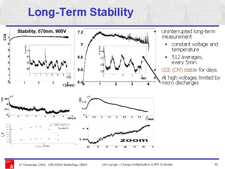
Long-Term Stability § § § 17 November 2009, 15 th RD 50 Workshop, CERN Uninterrupted long-term measurement § constant voltage and temperature § 512 averages, every 5 min CCE (CM) stable for days At high voltages limited by micro discharges Jörn Lange – Charge multiplication in EPI Si diodes 10

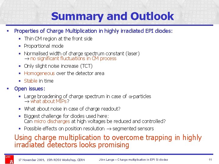
Summary and Outlook § Properties of Charge Multiplication in highly irradiated EPI diodes: § Thin CM region at the front side § Proportional mode § Normalised width of charge spectrum constant (laser) no significant fluctuations in CM process § Only slight noise increase (TCT) § Homogeneous over the detector area § Stable in time § Open issues: § Large broadening of charge spectrum in case of a-particles what about MIPs? § What about noise in case of charge readout? § Biggest challenge for diodes used here: Can micro discharges at high voltages be reduced and controlled? § Possible effects on position resolution segmented sensors Using charge multiplication to overcome trapping in highly irradiated detectors looks promising 17 November 2009, 15 th RD 50 Workshop, CERN Jörn Lange – Charge multiplication in EPI Si diodes 11

BACKUP SLIDES 17 November 2009, 15 th RD 50 Workshop, CERN Jörn Lange – Charge multiplication in EPI Si diodes 12

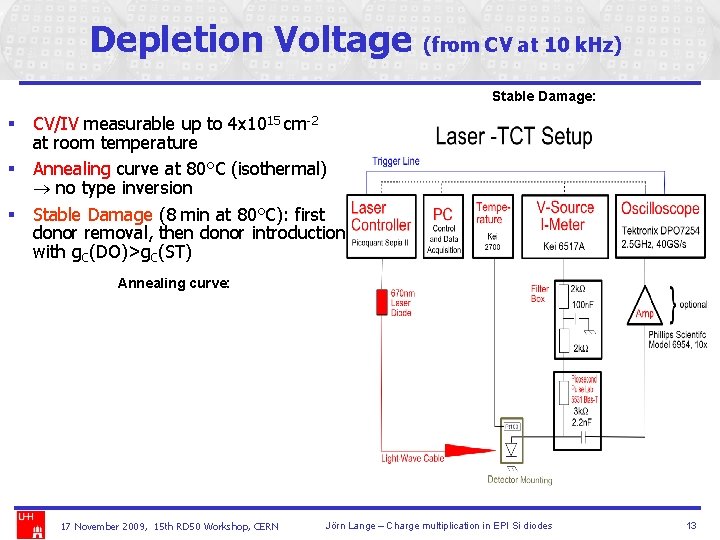
Depletion Voltage (from CV at 10 k. Hz) Stable Damage: § CV/IV measurable up to 4 x 1015 cm-2 at room temperature § Annealing curve at 80°C (isothermal) no type inversion § Stable Damage (8 min at 80°C): first donor removal, then donor introduction with g. C(DO)>g. C(ST) Annealing curve: 17 November 2009, 15 th RD 50 Workshop, CERN Jörn Lange – Charge multiplication in EPI Si diodes 13

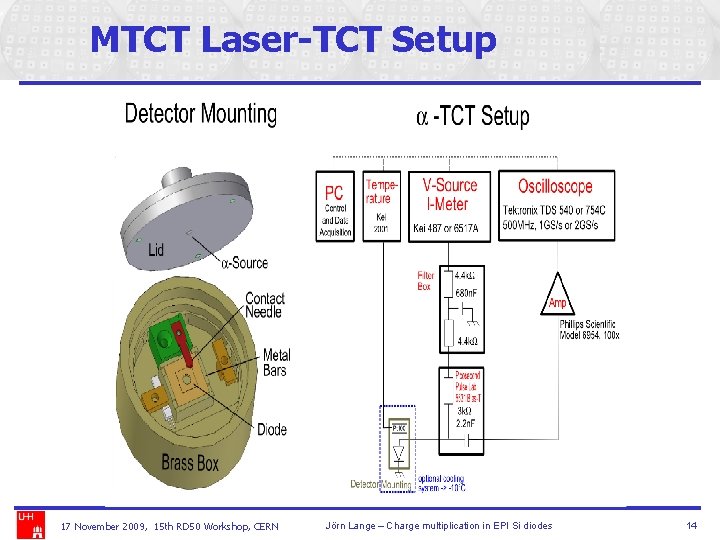
MTCT Laser-TCT Setup 17 November 2009, 15 th RD 50 Workshop, CERN Jörn Lange – Charge multiplication in EPI Si diodes 14

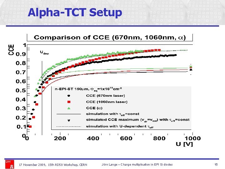
Alpha-TCT Setup 17 November 2009, 15 th RD 50 Workshop, CERN Jörn Lange – Charge multiplication in EPI Si diodes 15

17 November 2009, 15 th RD 50 Workshop, CERN Jörn Lange – Charge multiplication in EPI Si diodes 16