8 april 2015 FCPPL 2015 workshop HefeiChina P
- Slides: 35

8 april 2015 FCPPL 2015 workshop - Hefei/China - P. Pangaud 1 REVIEW OF THE ATLAS SILICON DETECTOR R&D PROJECT WORK FCPPL 2015 — Heife, CHINA Patrick Pangaud — CPPM 8 April 2015 On behalf of the Silicon detector FCPPL project

8 april 2015 FCPPL 2015 workshop - Hefei/China - P. Pangaud 2 CPPM / Atlas Chinese Cluster Collaboration • CPPM / ACC collaboration for design and test of Front-End pixel electronics for ATLAS phase II upgrade. • Scientific cooperation supervised by Pr. Xinchou LOU, Dr. Zheng WANG and Dr. Alexander ROZANOV, derived from ATLAS CPPM / ACC project (Pr. Shan JIN / Dr. Emmanuel MONNIER). • Co-Ph. D Jian Liu (SDU – Pr. Meng WANG / CPPM – Pr. Marlon BARBERO & Dr. Alexander ROZANOV). • The last development topics involve: • The investigation of technology access via SMIC foundry in China. Wei WEI (IHEP). • The tests and simulation in several HV CMOS technology. Jian Liu (SDU /CPPM).

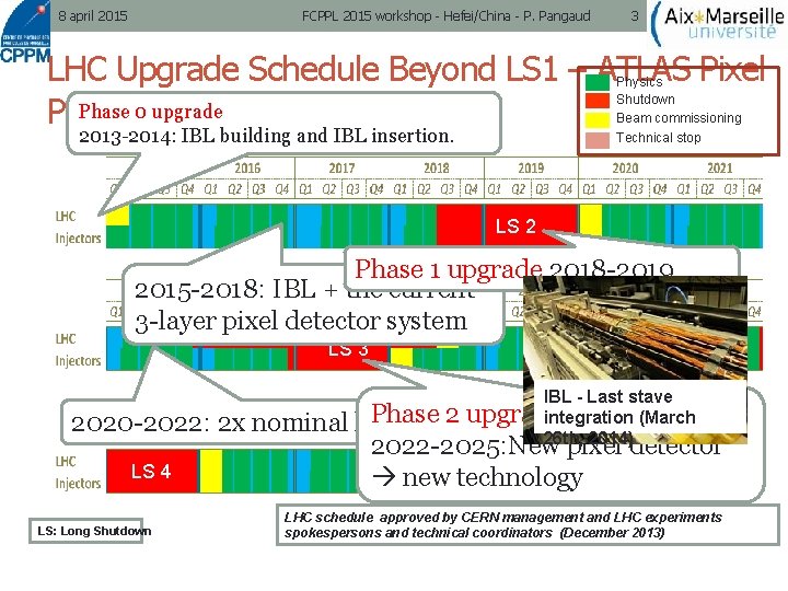
8 april 2015 FCPPL 2015 workshop - Hefei/China - P. Pangaud 3 LHC Upgrade Schedule Beyond LS 1 – ATLAS Pixel Phase 0 upgrade Perspective Physics Shutdown Beam commissioning Technical stop 2013 -2014: IBL building and IBL insertion. LS 2 Phase 1 upgrade 2018 -2019 2015 -2018: IBL + the current 3 -layer pixel detector system LS 3 2020 -2022: 2 x nominal LS 4 LS: Long Shutdown IBL - Last stave Phase 2 upgrade integration (March luminosity 26 th, 2014) 2022 -2025: New pixel detector LS 5 new technology LHC schedule approved by CERN management and LHC experiments spokespersons and technical coordinators (December 2013)

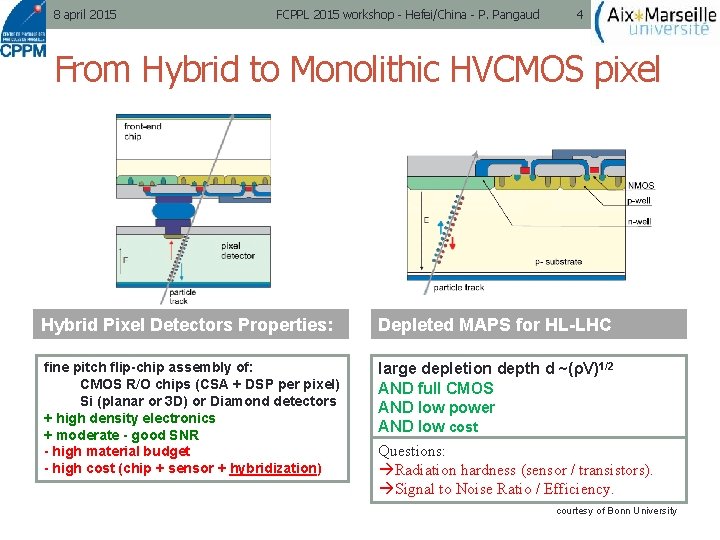
8 april 2015 FCPPL 2015 workshop - Hefei/China - P. Pangaud 4 From Hybrid to Monolithic HVCMOS pixel Hybrid Pixel Detectors Properties: Depleted MAPS for HL-LHC needed: fine pitch flip-chip assembly of: CMOS R/O chips (CSA + DSP per pixel) Si (planar or 3 D) or Diamond detectors + high density electronics + moderate - good SNR - high material budget - high cost (chip + sensor + hybridization) large depletion depth d ~(ρV)1/2 AND full CMOS AND low power AND low cost Questions: Radiation hardness (sensor / transistors). Signal to Noise Ratio / Efficiency. courtesy of Bonn University

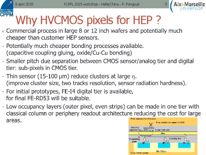
8 april 2015 FCPPL 2015 workshop - Hefei/China - P. Pangaud Why HVCMOS pixels for HEP ? • 5

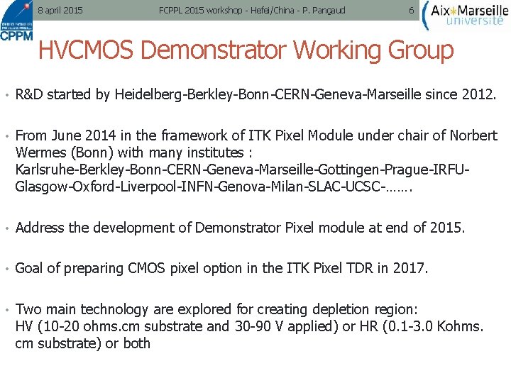
8 april 2015 FCPPL 2015 workshop - Hefei/China - P. Pangaud 6 HVCMOS Demonstrator Working Group • R&D started by Heidelberg-Berkley-Bonn-CERN-Geneva-Marseille since 2012. • From June 2014 in the framework of ITK Pixel Module under chair of Norbert Wermes (Bonn) with many institutes : Karlsruhe-Berkley-Bonn-CERN-Geneva-Marseille-Gottingen-Prague-IRFUGlasgow-Oxford-Liverpool-INFN-Genova-Milan-SLAC-UCSC-……. • Address the development of Demonstrator Pixel module at end of 2015. • Goal of preparing CMOS pixel option in the ITK Pixel TDR in 2017. • Two main technology are explored for creating depletion region: HV (10 -20 ohms. cm substrate and 30 -90 V applied) or HR (0. 1 -3. 0 Kohms. cm substrate) or both

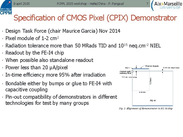
8 april 2015 FCPPL 2015 workshop - Hefei/China - P. Pangaud 7 Specification of CMOS Pixel (CPIX) Demonstrator • Design Task Force (chair Maurice Garcia) Nov 2014 • Pixel module of 1 -2 cm 2 • Radiation tolerance more than 50 MRads TID and 10 15 neq. cm-2 NIEL • Readout by the FE-I 4 chip • When possible also standalone readout • Power less than 20 µA/pixel • In-time efficiency more 95% after irradiation • Bondable either by bumps or glue to FE-I 4 with capacitive coupling • Pin-out compatibility of demonstrators in different technologies for test by many groups

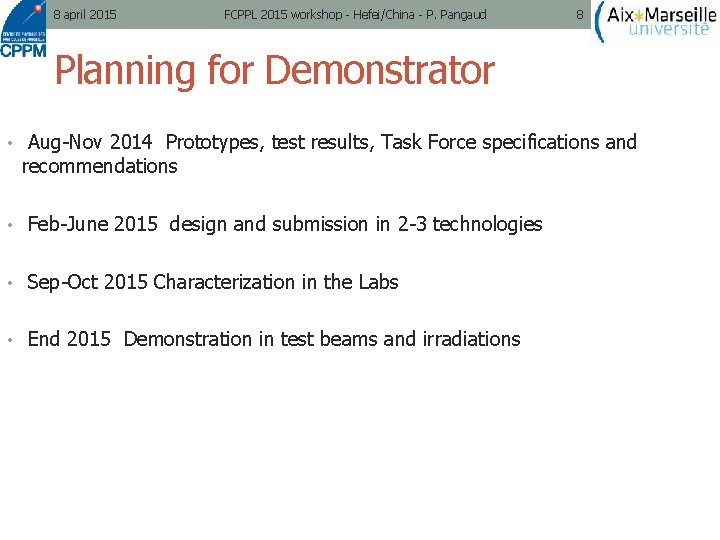
8 april 2015 FCPPL 2015 workshop - Hefei/China - P. Pangaud 8 Planning for Demonstrator • Aug-Nov 2014 Prototypes, test results, Task Force specifications and recommendations • Feb-June 2015 design and submission in 2 -3 technologies • Sep-Oct 2015 Characterization in the Labs • End 2015 Demonstration in test beams and irradiations

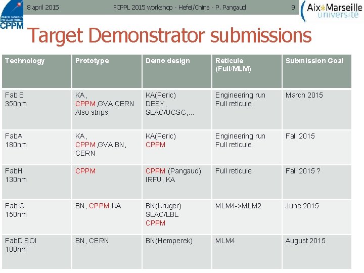
FCPPL 2015 workshop - Hefei/China - P. Pangaud 8 april 2015 9 Target Demonstrator submissions Technology Prototype Demo design Reticule (Full/MLM) Submission Goal Fab B 350 nm KA, CPPM, GVA, CERN Also strips KA(Peric) DESY, SLAC/UCSC, … Engineering run Full reticule March 2015 Fab. A 180 nm KA, CPPM, GVA, BN, CERN KA(Peric) CPPM Engineering run Full reticule Fall 2015 Fab. H 130 nm CPPM (Pangaud) IRFU, KA Full reticule Fall 2015 ? Fab G 150 nm BN, CPPM, KA BN(Kruger) SLAC/LBL CPPM MLM 4 ->MLM 2 June 2015 Fab. D SOI 180 nm BN, CERN BN(Hemperek) MLM 4 August 2015

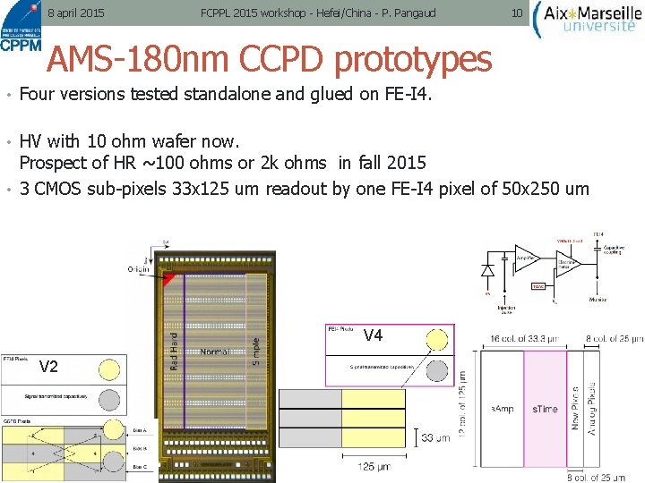
8 april 2015 FCPPL 2015 workshop - Hefei/China - P. Pangaud 10 AMS-180 nm CCPD prototypes • Four versions tested standalone and glued on FE-I 4. • HV with 10 ohm wafer now. Prospect of HR ~100 ohms or 2 k ohms in fall 2015 • 3 CMOS sub-pixels 33 x 125 um readout by one FE-I 4 pixel of 50 x 250 um V 4 V 2

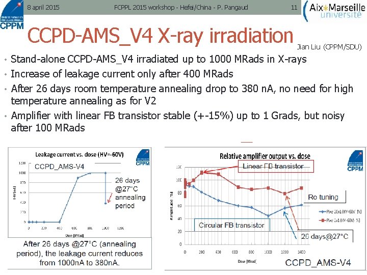
8 april 2015 FCPPL 2015 workshop - Hefei/China - P. Pangaud 11 CCPD-AMS_V 4 X-ray irradiation Jian Liu (CPPM/SDU) • Stand-alone CCPD-AMS_V 4 irradiated up to 1000 MRads in X-rays • Increase of leakage current only after 400 MRads • After 26 days room temperature annealing drop to 380 n. A, no need for high temperature annealing as for V 2 • Amplifier with linear FB transistor stable (+-15%) up to 1 Grads, but noisy after 100 MRads

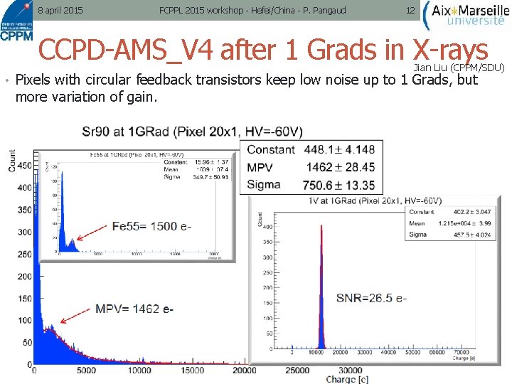
8 april 2015 FCPPL 2015 workshop - Hefei/China - P. Pangaud 12 CCPD-AMS_V 4 after 1 Grads in X-rays Jian Liu (CPPM/SDU) • Pixels with circular feedback transistors keep low noise up to 1 Grads, but more variation of gain.

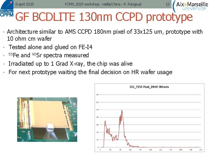
8 april 2015 FCPPL 2015 workshop - Hefei/China - P. Pangaud 13 GF BCDLITE 130 nm CCPD prototype • Architecture similar to AMS CCPD 180 nm pixel of 33 x 125 um, prototype with • • 10 ohm cm wafer Tested alone and glued on FE-I 4 55 Fe and 90 Sr spectra measured Irradiated up to 1 Grad X-ray, the chip was alive For next prototype waiting the final decision on HR wafer usage

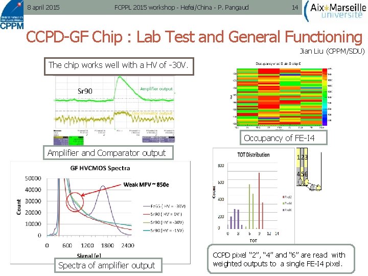
8 april 2015 FCPPL 2015 workshop - Hefei/China - P. Pangaud 14 CCPD-GF Chip : Lab Test and General Functioning Jian Liu (CPPM/SDU) The chip works well with a HV of -30 V. Occupancy of FE-I 4 Amplifier and Comparator output Spectra of amplifier output CCPD pixel “ 2”, “ 4” and “ 6” are read with weighted outputs to a single FE-I 4 pixel.

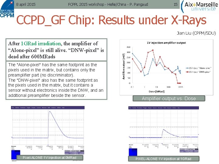
8 april 2015 FCPPL 2015 workshop - Hefei/China - P. Pangaud 15 CCPD_GF Chip: Results under X-Rays Jian Liu (CPPM/SDU) After 1 GRad irradiation, the amplifier of “Alone-pixel” is still alive. “DNW-pixel” is dead after 600 MRads The "Alone-pixel" has the same footprint as the pixels used in the matrix, but contains only the preamplifier part (no discriminator). The "DNW-pixel" also has the same footprint as the pixels used in the matrix, but it contains a sensor without electronics inside the DNW, and an additional preamplifier beside the sensor. Pixel-ALONE 1 V injection at 0 MRad Amplifier output vs. Dose PIXEL-ALONE 1 V injection at 1 GRad

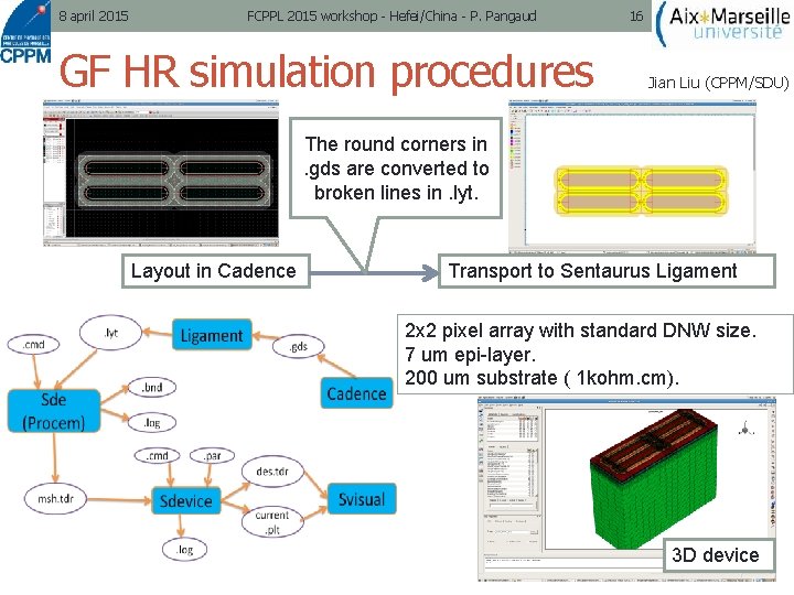
8 april 2015 FCPPL 2015 workshop - Hefei/China - P. Pangaud GF HR simulation procedures 16 Jian Liu (CPPM/SDU) The round corners in. gds are converted to broken lines in. lyt. Layout in Cadence Transport to Sentaurus Ligament 2 x 2 pixel array with standard DNW size. 7 um epi-layer. 200 um substrate ( 1 kohm. cm). 3 D device

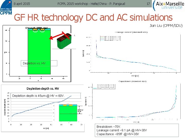
8 april 2015 FCPPL 2015 workshop - Hefei/China - P. Pangaud 17 GF HR technology DC and AC simulations Jian Liu (CPPM/SDU) Depletion vs. HV Depletion depth is 45 um @ HV =-60 V. Breakdown ~70 V. Leakage current ~9. 1 p. A @ HV=30 V Capacitance ~85 f. F @ HV=30 V

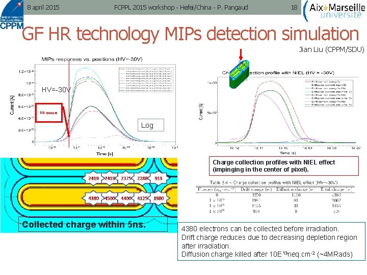
8 april 2015 FCPPL 2015 workshop - Hefei/China - P. Pangaud 18 GF HR technology MIPs detection simulation Jian Liu (CPPM/SDU) HV=-30 V Hit occurs Log Charge collection profiles with NIEL effect (impinging in the center of pixel). Collected charge within 5 ns. 4380 electrons can be collected before irradiation. Drift charge reduces due to decreasing depletion region after irradiation. Diffusion charge killed after 10 E 13 neq. cm-2 (~4 MRads)

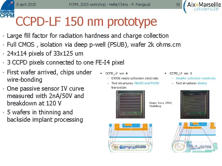
8 april 2015 FCPPL 2015 workshop - Hefei/China - P. Pangaud 19 CCPD-LF 150 nm prototype • Large fill factor for radiation hardness and charge collection • Full CMOS , isolation via deep p-well (PSUB), wafer 2 k ohms. cm • 24 x 114 pixels of 33 x 125 um • 3 CCPD pixels connected to one FE-I 4 pixel • First wafer arrived, chips under wire-bonding • One passive sensor IV curve measured with 2 n. A/50 V and breakdown at 120 V • 5 wafers in thinning and backside implant processing

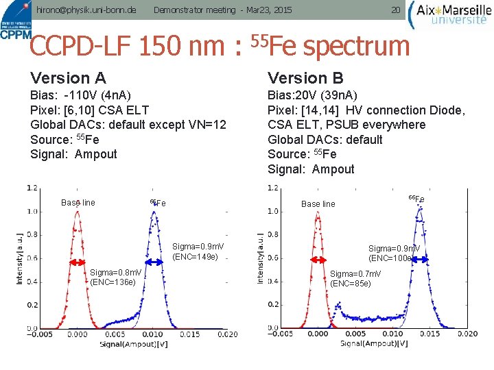
hirono@physik. uni-bonn. de Demonstrator meeting - Mar 23, 2015 20 CCPD-LF 150 nm : 55 Fe spectrum Version A Version B Bias: -110 V (4 n. A) Pixel: [6, 10] CSA ELT Global DACs: default except VN=12 Source: 55 Fe Signal: Ampout Bias: 20 V (39 n. A) Pixel: [14, 14] HV connection Diode, CSA ELT, PSUB everywhere Global DACs: default Source: 55 Fe Signal: Ampout Base line 55 Fe Sigma=0. 9 m. V (ENC=149 e) Sigma=0. 8 m. V (ENC=136 e) 55 Fe Base line Sigma=0. 9 m. V (ENC=100 e) Sigma=0. 7 m. V (ENC=85 e)

8 april 2015 FCPPL 2015 workshop - Hefei/China - P. Pangaud 21 Conclusions and future plans • HVCMOS pixel prototypes produced in 8 different technologies. We have the choice… • Most advanced CCPD test beam results in AMS 180 nm technologies results 99. 7% efficiency before radiations. The CCPD_AMS_V 4 chip is still alive after radiations up to 1 Grads. Timing to be improved (lower thresholds, higher signals with HR, time slewing corrections). • Very promising results with the LFoundry technology. • TCAD simulation, a very good help addressed to the HVCMOS project. Thanks for the Jian Lu (CPPM/SDU) contribution and work through his Co-Ph. D. • CMOS Demonstrator program started with the goal to produce 2 -3 demonstrator types for test beam in the fall of 2015. • The IHEP and CPPM have a very strong collaboration since many years, on ATLAS developments. We are expanding the partnership between Chinese institutes and CPPM on HVCMOS development by adding the SMIC foundry for the evaluation and testing.

8 april 2015 FCPPL 2015 workshop - Hefei/China - P. Pangaud BACKUP 22

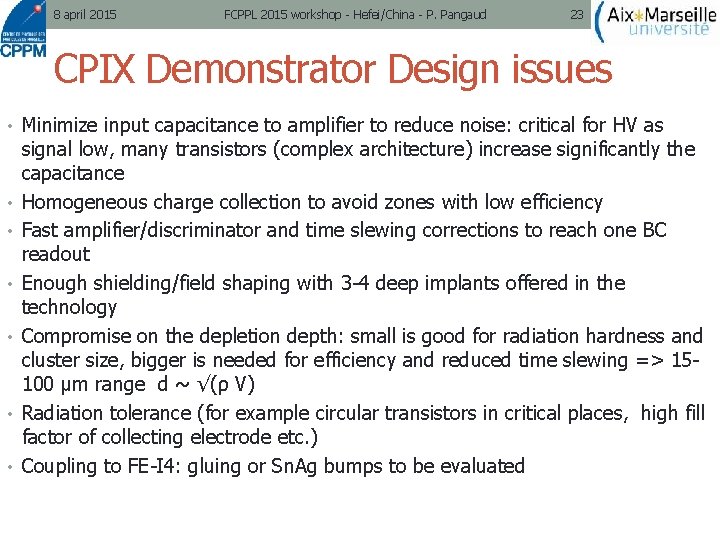
8 april 2015 FCPPL 2015 workshop - Hefei/China - P. Pangaud 23 CPIX Demonstrator Design issues • Minimize input capacitance to amplifier to reduce noise: critical for HV as • • • signal low, many transistors (complex architecture) increase significantly the capacitance Homogeneous charge collection to avoid zones with low efficiency Fast amplifier/discriminator and time slewing corrections to reach one BC readout Enough shielding/field shaping with 3 -4 deep implants offered in the technology Compromise on the depletion depth: small is good for radiation hardness and cluster size, bigger is needed for efficiency and reduced time slewing => 15100 µm range d ~ √(ρ V) Radiation tolerance (for example circular transistors in critical places, high fill factor of collecting electrode etc. ) Coupling to FE-I 4: gluing or Sn. Ag bumps to be evaluated

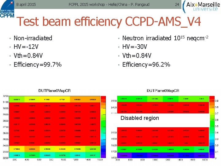
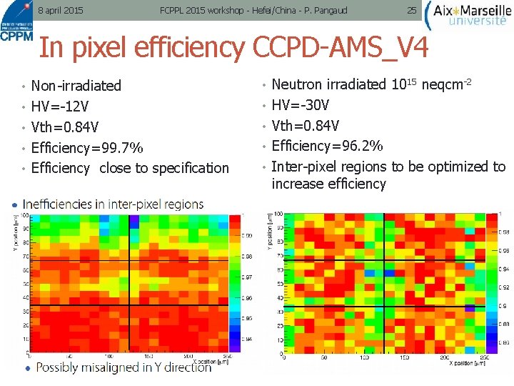
8 april 2015 FCPPL 2015 workshop - Hefei/China - P. Pangaud 24 Test beam efficiency CCPD-AMS_V 4 • Non-irradiated • Neutron irradiated 1015 neqcm-2 • HV=-12 V • HV=-30 V • Vth=0. 84 V • Efficiency=99. 7% • Efficiency=96. 2% Disabled region

8 april 2015 FCPPL 2015 workshop - Hefei/China - P. Pangaud 25 In pixel efficiency CCPD-AMS_V 4 • Non-irradiated • Neutron irradiated 1015 neqcm-2 • HV=-12 V • HV=-30 V • Vth=0. 84 V • Efficiency=99. 7% • Efficiency=96. 2% • Efficiency close to specification • Inter-pixel regions to be optimized to increase efficiency

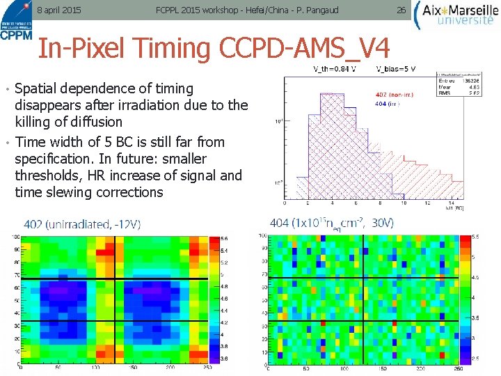
8 april 2015 FCPPL 2015 workshop - Hefei/China - P. Pangaud In-Pixel Timing CCPD-AMS_V 4 • Spatial dependence of timing disappears after irradiation due to the killing of diffusion • Time width of 5 BC is still far from specification. In future: smaller thresholds, HR increase of signal and time slewing corrections 26

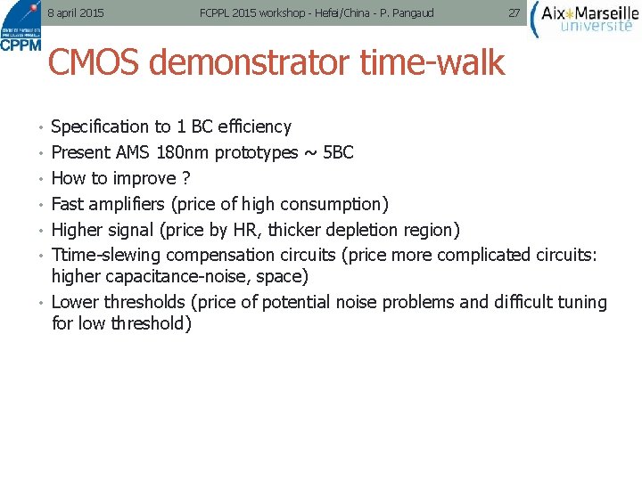
8 april 2015 FCPPL 2015 workshop - Hefei/China - P. Pangaud 27 CMOS demonstrator time-walk • Specification to 1 BC efficiency • Present AMS 180 nm prototypes ~ 5 BC • How to improve ? • Fast amplifiers (price of high consumption) • Higher signal (price by HR, thicker depletion region) • Ttime-slewing compensation circuits (price more complicated circuits: higher capacitance-noise, space) • Lower thresholds (price of potential noise problems and difficult tuning for low threshold)

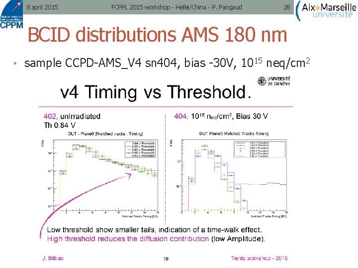
8 april 2015 FCPPL 2015 workshop - Hefei/China - P. Pangaud 28 BCID distributions AMS 180 nm • sample CCPD-AMS_V 4 sn 404, bias -30 V, 1015 neq/cm 2

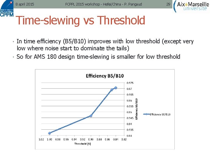
8 april 2015 FCPPL 2015 workshop - Hefei/China - P. Pangaud 29 Time-slewing vs Threshold • In time efficiency (B 5/B 10) improves with low threshold (except very low where noise start to dominate the tails) • So for AMS 180 design time-slewing is smaller for low threshold

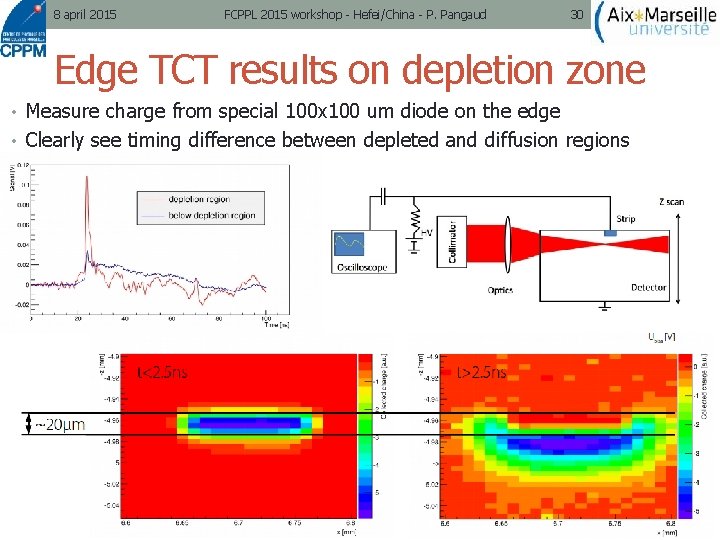
8 april 2015 FCPPL 2015 workshop - Hefei/China - P. Pangaud 30 Edge TCT results on depletion zone • Measure charge from special 100 x 100 um diode on the edge • Clearly see timing difference between depleted and diffusion regions

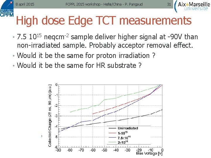
8 april 2015 FCPPL 2015 workshop - Hefei/China - P. Pangaud 31 High dose Edge TCT measurements • 7. 5 1015 neqcm-2 sample deliver higher signal at -90 V than non-irradiated sample. Probably acceptor removal effect. • Would it be the same for proton irradiation ? • Would it be the same for HR substrate ?

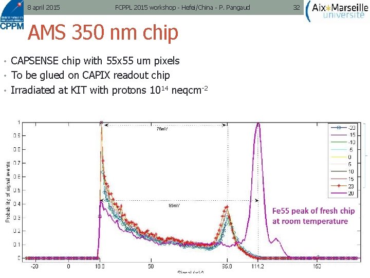
8 april 2015 FCPPL 2015 workshop - Hefei/China - P. Pangaud AMS 350 nm chip • CAPSENSE chip with 55 x 55 um pixels • To be glued on CAPIX readout chip • Irradiated at KIT with protons 1014 neqcm-2 32

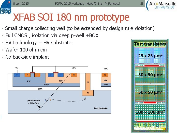
8 april 2015 FCPPL 2015 workshop - Hefei/China - P. Pangaud 33 XFAB SOI 180 nm prototype • Small charge collecting well (to be extended by design rule violation) • Full CMOS , isolation via deep p-well +BOX • HV technology + HR substrate • Wafer 100 ohm cm • No backside implant

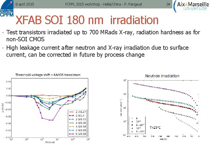
8 april 2015 FCPPL 2015 workshop - Hefei/China - P. Pangaud 34 XFAB SOI 180 nm irradiation • Test transistors irradiated up to 700 MRads X-ray, radiation hardness as for non-SOI CMOS • High leakage current after neutron and X-ray irradiation due to surface current, can be corrected in future by process change

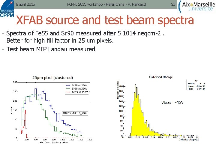
8 april 2015 FCPPL 2015 workshop - Hefei/China - P. Pangaud 35 XFAB source and test beam spectra • Spectra of Fe 55 and Sr 90 measured after 5 1014 neqcm-2. Better for high fill factor in 25 um pixels. • Test beam MIP Landau measured