2010 RE Computer System Education Research Lecture 9
- Slides: 21
2010 R&E Computer System Education & Research Lecture 9. MIPS Processor Design – Instruction Fetch Prof. Taeweon Suh Computer Science Education Korea University
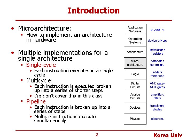
Introduction • Microarchitecture: § How to implement an architecture in hardware • Multiple implementations for a single architecture § Single-cycle • Each instruction executes in a single cycle § Multicycle • Each instruction is executed broken up into a series of shorter steps • We don’t cover this in this class § Pipeline • Each instruction is broken up into a series of steps • Multiple instructions execute simultaneously 2 Korea Univ
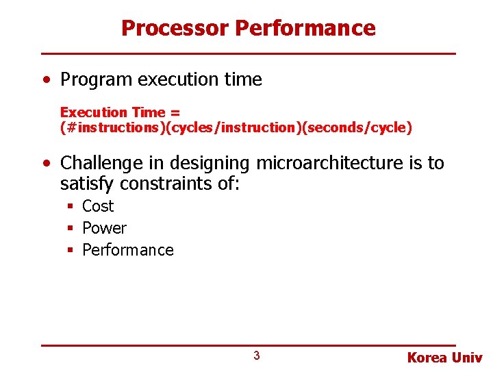
Processor Performance • Program execution time Execution Time = (#instructions)(cycles/instruction)(seconds/cycle) • Challenge in designing microarchitecture is to satisfy constraints of: § Cost § Power § Performance 3 Korea Univ
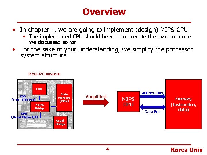
Overview • In chapter 4, we are going to implement (design) MIPS CPU § The implemented CPU should be able to execute the machine code we discussed so far • For the sake of your understanding, we simplify the processor system structure Real-PC system CPU FSB (Front-Side Bus) Main Memory (DDR) Address Bus Simplified MIPS CPU North Bridge Data Bus DMI (Direct Media I/F) Memory (Instruction, data) South Bridge 4 Korea Univ
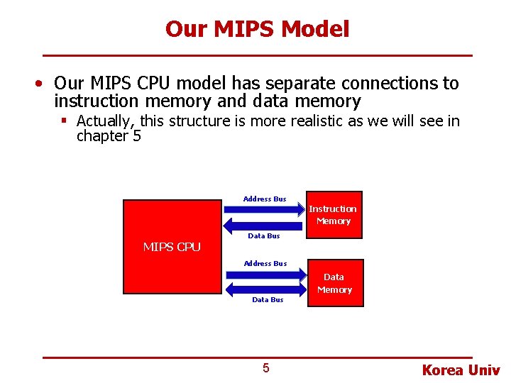
Our MIPS Model • Our MIPS CPU model has separate connections to instruction memory and data memory § Actually, this structure is more realistic as we will see in chapter 5 Address Bus Instruction Memory MIPS CPU Data Bus Address Bus Data Memory Data Bus 5 Korea Univ
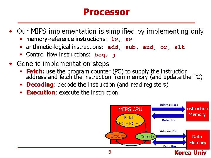
Processor • Our MIPS implementation is simplified by implementing only § memory-reference instructions: lw, sw § arithmetic-logical instructions: add, sub, and, or, slt § Control flow instructions: beq, j • Generic implementation steps § Fetch: use the program counter (PC) to supply the instruction address and fetch the instruction from memory (and update the PC) § Decoding: decode the instruction (and read registers) § Execution: execute the instruction MIPS CPU Fetch PC = PC +4 Address Bus Instruction Memory Data Bus Address Bus Execute Decode Data Bus 6 Data Memory Korea Univ
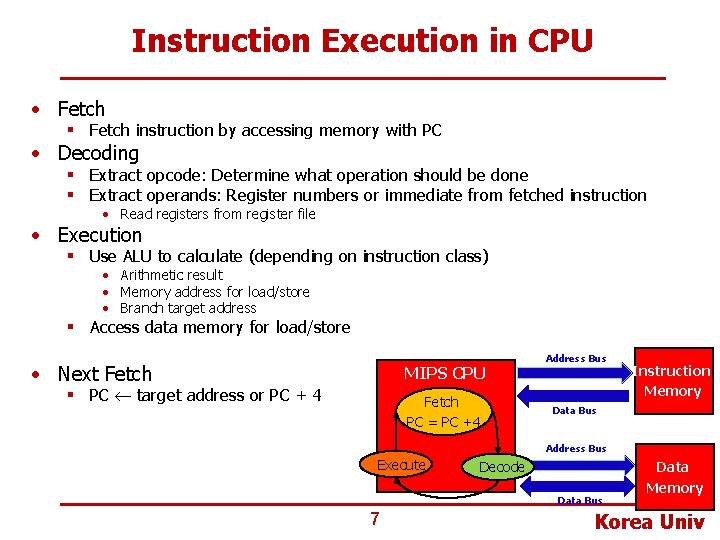
Instruction Execution in CPU • Fetch § Fetch instruction by accessing memory with PC • Decoding § Extract opcode: Determine what operation should be done § Extract operands: Register numbers or immediate from fetched instruction • Read registers from register file • Execution § Use ALU to calculate (depending on instruction class) • Arithmetic result • Memory address for load/store • Branch target address § Access data memory for load/store • Next Fetch MIPS CPU § PC target address or PC + 4 Fetch PC = PC +4 Address Bus Instruction Memory Data Bus Address Bus Execute Decode Data Bus 7 Data Memory Korea Univ
Revisiting Logic Design Basics • Combinational logic § Output is directly determined by input • Sequential logic § Output is determined not only by input, but also by internal state § Sequential logic needs state elements to store information • Flip-flop and latch are used to store the state information § But, avoid using latch in digital design 8 Korea Univ
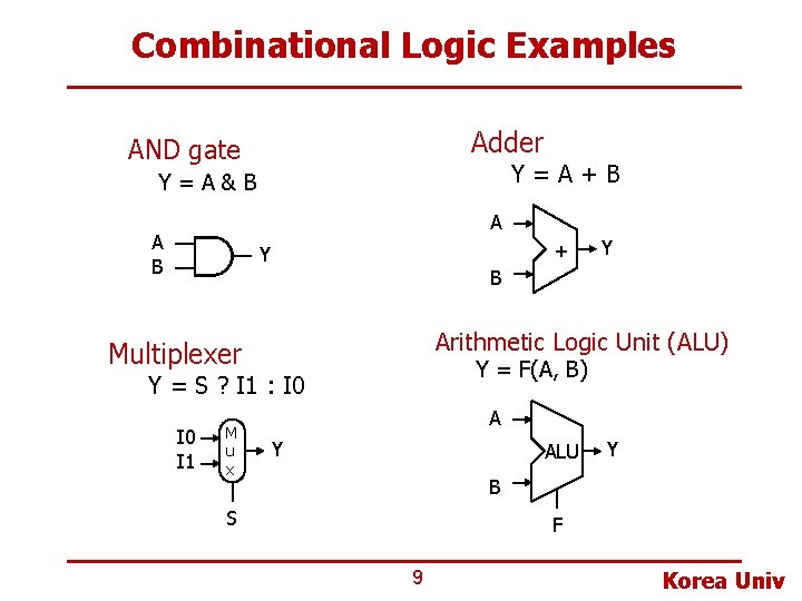
Combinational Logic Examples Adder AND gate Y=A+B Y=A&B A A B + Y B Arithmetic Logic Unit (ALU) Multiplexer Y = F(A, B) Y = S ? I 1 : I 0 I 1 M u x Y ALU Y B S F 9 Korea Univ
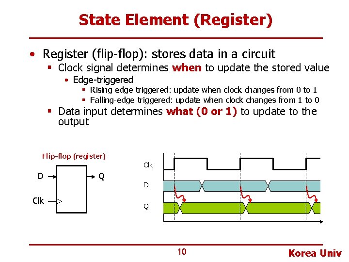
State Element (Register) • Register (flip-flop): stores data in a circuit § Clock signal determines when to update the stored value • Edge-triggered § Rising-edge triggered: update when clock changes from 0 to 1 § Falling-edge triggered: update when clock changes from 1 to 0 § Data input determines what (0 or 1) to update to the output Flip-flop (register) Clk D Clk Q D Q 10 Korea Univ
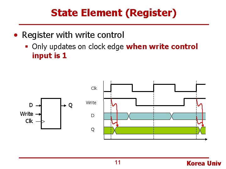
State Element (Register) • Register with write control § Only updates on clock edge when write control input is 1 Clk D Write Clk Q Write D Q 11 Korea Univ
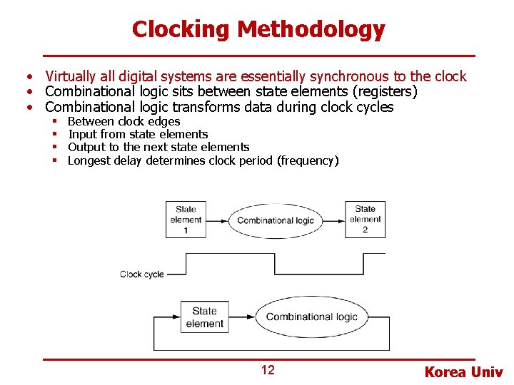
Clocking Methodology • Virtually all digital systems are essentially synchronous to the clock • Combinational logic sits between state elements (registers) • Combinational logic transforms data during clock cycles § § Between clock edges Input from state elements Output to the next state elements Longest delay determines clock period (frequency) 12 Korea Univ
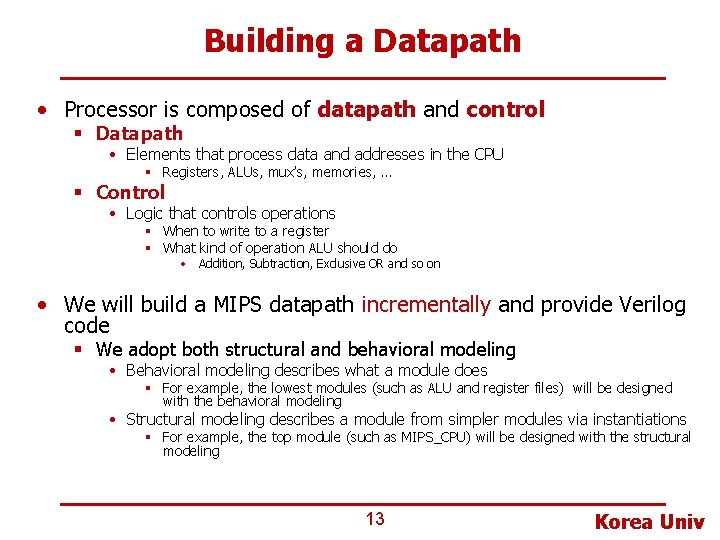
Building a Datapath • Processor is composed of datapath and control § Datapath • Elements that process data and addresses in the CPU § Registers, ALUs, mux’s, memories, … § Control • Logic that controls operations § When to write to a register § What kind of operation ALU should do • Addition, Subtraction, Exclusive OR and so on • We will build a MIPS datapath incrementally and provide Verilog code § We adopt both structural and behavioral modeling • Behavioral modeling describes what a module does § For example, the lowest modules (such as ALU and register files) will be designed with the behavioral modeling • Structural modeling describes a module from simpler modules via instantiations § For example, the top module (such as MIPS_CPU) will be designed with the structural modeling 13 Korea Univ
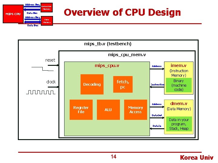
Address Bus MIPS CPU Instruction Memory Data Bus Address Bus Overview of CPU Design Data Memory Data Bus mips_tb. v (testbench) mips_cpu_mem. v reset mips_cpu. v Address imem. v (Instruction Memory) clock fetch, pc Decoding Register File ALU Memory Access Instruction Address dmem. v (Data Memory) Data. Out Data. In 14 Binary (machine code) Data in your program, Stack, Heap Korea Univ
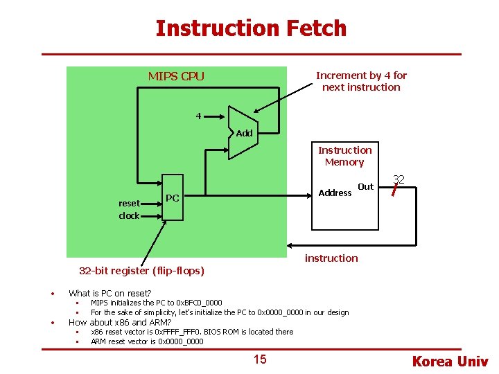
Instruction Fetch MIPS CPU Increment by 4 for next instruction 4 Add Instruction Memory reset clock Address PC Out 32 instruction 32 -bit register (flip-flops) • • What is PC on reset? § § MIPS initializes the PC to 0 x. BFC 0_0000 For the sake of simplicity, let’s initialize the PC to 0 x 0000_0000 in our design § § x 86 reset vector is 0 x. FFFF_FFF 0. BIOS ROM is located there ARM reset vector is 0 x 0000_0000 How about x 86 and ARM? 15 Korea Univ
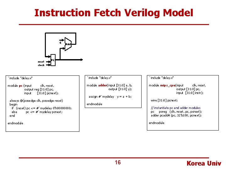
Instruction Fetch Verilog Model 4 reset clock Add PC `include "delay. v" module pc (input clk, reset, output reg [31: 0] pc, input [31: 0] pcnext); module adder(input [31: 0] a, b, output [31: 0] y); module mips_cpu(input clk, reset, output [31: 0] pc, input [31: 0] instr); always @(posedge clk, posedge reset) begin if (reset) pc <= #`mydelay 0'h 0000; else pc <= #`mydelay pcnext; end assign #`mydelay y = a + b; endmodule wire [31: 0] pcnext; // instantiate pc and adder modules pc pcreg (clk, reset, pcnext); adder pcadd 4 (pc, 32'b 100, pcnext); endmodule 16 Korea Univ
Memory • As studied in the Computer Logic Design, memory is classified into RAM (Random Access Memory) and ROM (Read-Only Memory) § RAM is classified into DRAM (Dynamic RAM) and SRAM (Static RAM) § DDR is a DRAM • Short form of DDR (Double Data Rate) SDRAM (Synchronous DRAM) § DDR is used as main memory in modern computers • We use a simple Verilog memory model that stores your program since our focus is on how CPU works 17 Korea Univ
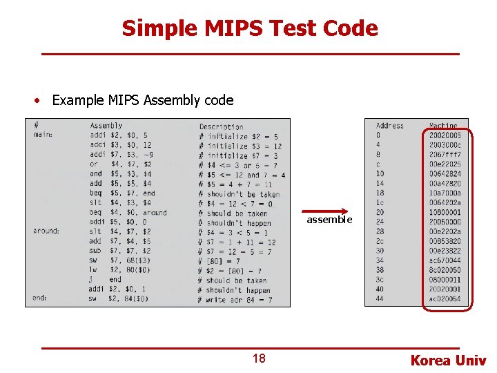
Simple MIPS Test Code • Example MIPS Assembly code assemble 18 Korea Univ
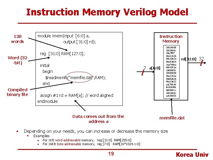
Instruction Memory Verilog Model module imem(input [6: 0] a, output [31: 0] rd); 128 words reg [31: 0] RAM[127: 0]; Word (32 -bit) Compiled binary file Instruction Memory initial begin $readmemh("memfile. dat", RAM); end 7 assign #1 rd = RAM[a]; // word aligned endmodule Data comes out from the address a • a[6: 0] 20020005 2003000 c 2067 fff 7 00 e 22025 00642824 00 a 42820 10 a 7000 a 0064202 a 10800001 20050000 00 e 2202 a 00853820 00 e 23822 ac 670044 8 c 020050 08000011 20020001 ac 020054 rd[31: 0] 32 memfile. dat Depending on your needs, you can increase or decrease the memory size § Examples • • For 1 KB word-addressable memory, reg [31: 0] RAM[255: 0] For 16 KB byte-addressable memory, reg [7: 0] RAM[16*1024 -1: 0] 19 Korea Univ
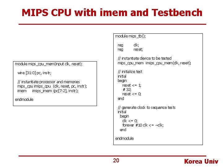
MIPS CPU with imem and Testbench module mips_tb(); reg module mips_cpu_mem(input clk, reset); wire [31: 0] pc, instr; // instantiate processor and memories mips_cpu imips_cpu (clk, reset, pc, instr); imem imips_imem (pc[7: 2], instr); endmodule clk; reset; // instantiate device to be tested mips_cpu_mem imips_cpu_mem(clk, reset); // initialize test initial begin reset <= 1; # 32; reset <= 0; end // generate clock to sequence tests initial begin clk <= 0; forever #10 clk <= ~clk; endmodule 20 Korea Univ
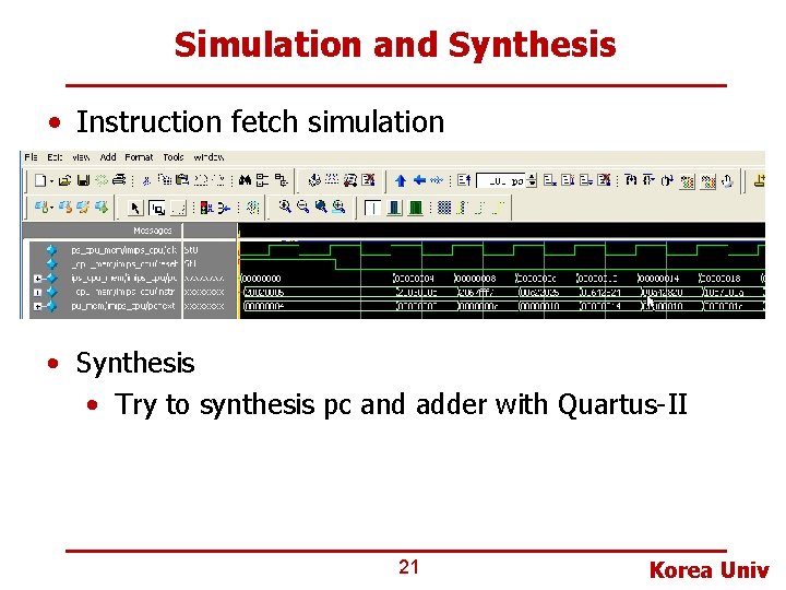
Simulation and Synthesis • Instruction fetch simulation • Synthesis • Try to synthesis pc and adder with Quartus-II 21 Korea Univ