www seattlenano org Lets ReviewWhat is Nanotech SHINE

- Slides: 8

www. seattlenano. org Let’s Review…What is Nanotech? SHINE: Seattle’s Hub for Industry-driven Nanotechnology Education

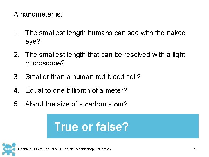
A nanometer is: 1. The smallest length humans can see with the naked eye? 2. The smallest length that can be resolved with a light microscope? 3. Smaller than a human red blood cell? 4. Equal to one billionth of a meter? 5. About the size of a carbon atom? True or false? Seattle’s Hub for Industry-Driven Nanotechnology Education 2

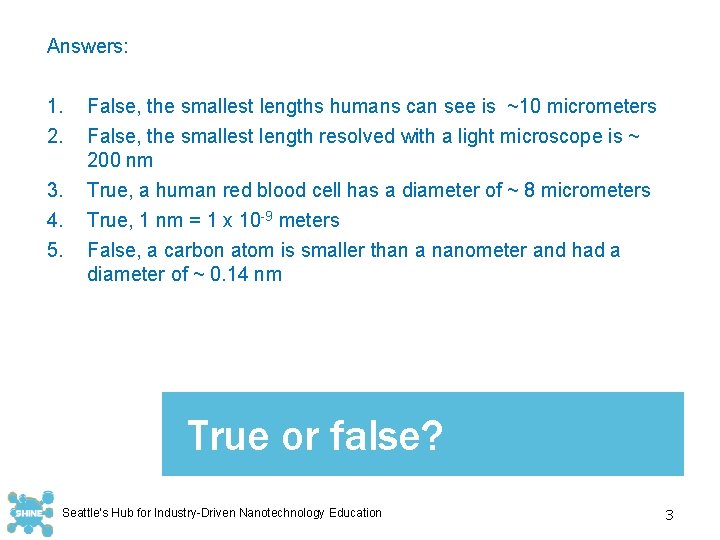
Answers: 1. 2. 3. 4. 5. False, the smallest lengths humans can see is ~10 micrometers False, the smallest length resolved with a light microscope is ~ 200 nm True, a human red blood cell has a diameter of ~ 8 micrometers True, 1 nm = 1 x 10 -9 meters False, a carbon atom is smaller than a nanometer and had a diameter of ~ 0. 14 nm True or false? Seattle’s Hub for Industry-Driven Nanotechnology Education 3

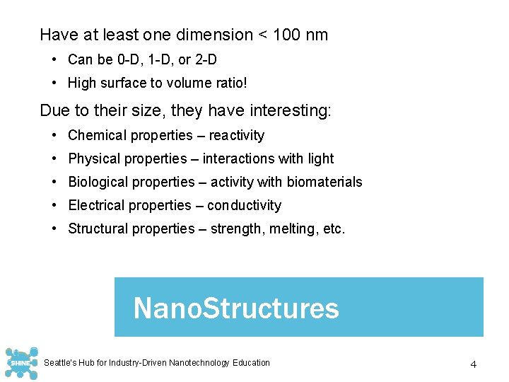
Have at least one dimension < 100 nm • Can be 0 -D, 1 -D, or 2 -D • High surface to volume ratio! Due to their size, they have interesting: • Chemical properties – reactivity • Physical properties – interactions with light • Biological properties – activity with biomaterials • Electrical properties – conductivity • Structural properties – strength, melting, etc. Nano. Structures Seattle’s Hub for Industry-Driven Nanotechnology Education 4

Many ways to make nanostructures • Bottom-up (chemistry) • Top-down (lithography) Many techniques are not unique to field • Some are centuries old! Some high-tech tools • May require cleanroom, vacuum systems, etc. Nano. Fabrication Seattle’s Hub for Industry-Driven Nanotechnology Education 5

Microscopes used to “see” nanostructures • use electrons (SEM and TEM) • use a scanning probe tip (AFM and STM) Some techniques not unique to nanotech • used to determine chemical structure, elemental analysis, etc. Nano. Characterization Seattle’s Hub for Industry-Driven Nanotechnology Education 6

Applications in nearly every industry: Electronics Medicine (diagnostics and treatment) Alternative energy (production and storage) Cosmetics Food Sporting goods Clothing Vehicles and aerospace Applications Seattle’s Hub for Industry-Driven Nanotechnology Education 7

To access additional educational resources please visit: www. seattlenano. org This material is based upon work supported by the National Science Foundation under Grant Number 1204279. Any opinions, findings, and conclusions or recommendations expressed in this material are those of the author(s) and do not necessarily reflect the views of the National Science Foundation. 8