University of Trieste Kolymvari Chania Crete Greece 11
![5/17 Why Ga. As/Al. Ga. As? Band gap [e. V] Atomic number Mobility of 5/17 Why Ga. As/Al. Ga. As? Band gap [e. V] Atomic number Mobility of](https://slidetodoc.com/presentation_image_h/264699b08978a8d31330d4f3bcecab30/image-5.jpg)
- Slides: 16

University of Trieste Kolymvari, Chania, Crete, Greece, 11. 07. 2019 Time response of avalanche photodiodes based on Ga. As/Al. Ga. As with separated absorption and multiplication region Tereza Steinhartova 1, 3, Camilla Nichetti 1, 2, Matias Antonelli 2, Giuseppe Cautero 2, 4, Dario De Angelis 1, Alessandro Pilotto 6, Francesco Driussi 6, Pierpaolo Palestri 6, Luca Selmi 7, Fulvia Arfelli 1, 4 , Giorgio Biasiol 3, Ralf Hendrik Menk 2, 4, 5 1. Department of Physics, University of Trieste, 34128 Trieste, Italy 2. Elettra-Sincrotrone Trieste S. C. p. A, Area Science Park Basovizza, 34149 Trieste, Italy. 3. IOM CNR, Laboratorio TASC, Area Science Park Basovizza, 34149 Trieste, Italy. 4. Istituto Nazionale di Fisica Nucleare, INFN Sezione di Trieste, 34100, Italy. 5. Department of Medical Imaging, University of Saskatchewan, Saskatoon, SK S 7 N 5 A 2, Canada. 6. DPIA, University of Udine, Via delle Scienze 206, 33100 Udine, Italy. 7. DIEF, University of Modena and Reggio Emilia, Via Trovarelli 2, 44100 Modena, Italy. PHD school in Nanotechnology

2/17 Outline • Motivation – Why Avalanche Photo. Diodes (APDs)? – Why Ga. As? – Why Molecular Beam Epitaxy? • Results − Response of 3 different types of devices to a pulsed green laser • Summary so far and what is next

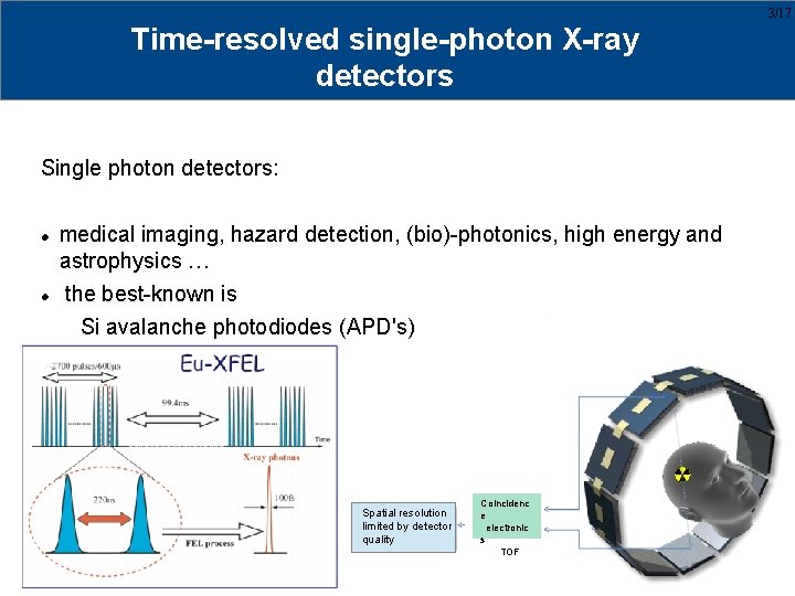
3/17 Time-resolved single-photon X-ray detectors Single photon detectors: medical imaging, hazard detection, (bio)-photonics, high energy and astrophysics … the best-known is Si avalanche photodiodes (APD's) Spatial resolution limited by detector quality Coincidenc e electronic s TOF

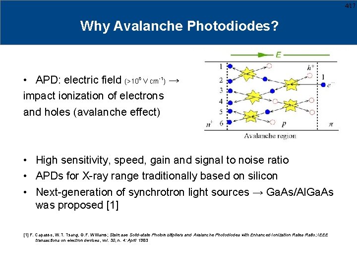
4/17 Why Avalanche Photodiodes? • APD: electric field (>105 V cm-1) → impact ionization of electrons and holes (avalanche effect) • High sensitivity, speed, gain and signal to noise ratio • APDs for X-ray range traditionally based on silicon • Next-generation of synchrotron light sources → Ga. As/Al. Ga. As was proposed [1] F. Capasso, W. T. Tsang, G. F. Williams; Staircase Solid-state Photomultipliers and Avalanche Photodiodes with Enhanced Ionization Rates Ratio; IEEE transactions on electron devices, vol. 30, n. 4: April 1983 4
![517 Why Ga AsAl Ga As Band gap e V Atomic number Mobility of 5/17 Why Ga. As/Al. Ga. As? Band gap [e. V] Atomic number Mobility of](https://slidetodoc.com/presentation_image_h/264699b08978a8d31330d4f3bcecab30/image-5.jpg)
5/17 Why Ga. As/Al. Ga. As? Band gap [e. V] Atomic number Mobility of e[cm 2/ (V⋅s)] Si 1. 1 14 ≤ 1400 Alx. Ga 1 - > 1. 4 31(Ga), 33(A ≤ 8500 Source of data: http: //henke. lbl. gov/optical_constants/ As Larger band gap → higher resistance to s) radiation damage, no cooling needed Band gap engineering: possibility to tailor material composition on nanoscale x Higher atomic number → higher absorbance compared to silicon Active absorption layer can be thinner → short pass time, faster devices 5 (for soft X-ray energies exceeding 11 ke. V absorption length is a factor of 22 shorter in Ga. As than in

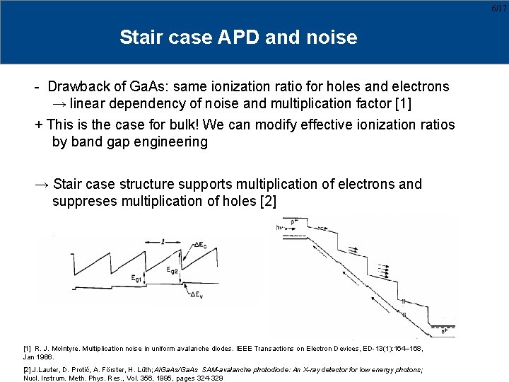
6/17 Stair case APD and noise - Drawback of Ga. As: same ionization ratio for holes and electrons → linear dependency of noise and multiplication factor [1] + This is the case for bulk! We can modify effective ionization ratios by band gap engineering → Stair case structure supports multiplication of electrons and suppreses multiplication of holes [2] [1] R. J. Mc. Intyre. Multiplication noise in uniform avalanche diodes. IEEE Transactions on Electron Devices, ED-13(1): 164– 168, Jan 1966. 6 [2] J. Lauter, D. Protić, A. Förster, H. Lüth; Al. Ga. As/Ga. As SAM-avalanche photodiode: An X-ray detector for low energy photons; Nucl. Instrum. Meth. Phys. Res. , Vol. 356, 1995, pages 324 -329

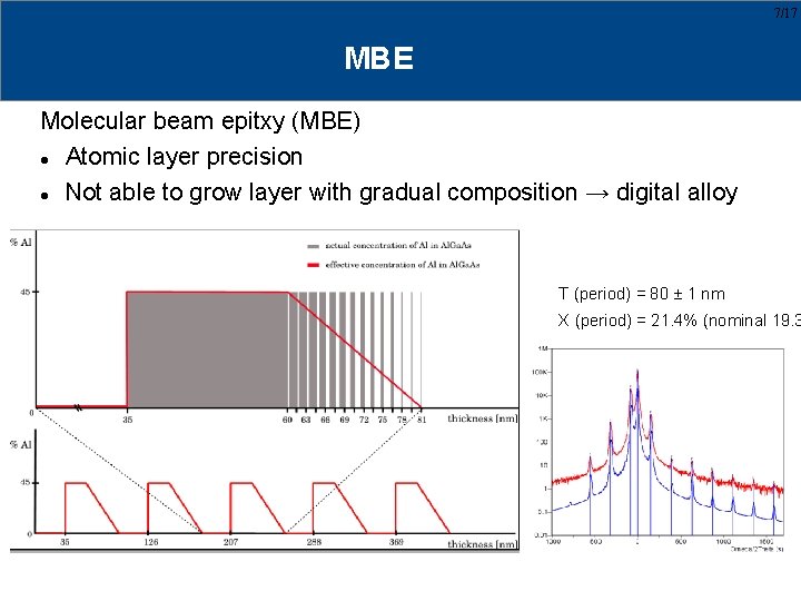
7/17 MBE Molecular beam epitxy (MBE) Atomic layer precision Not able to grow layer with gradual composition → digital alloy T (period) = 80 ± 1 nm X (period) = 21. 4% (nominal 19. 3 7

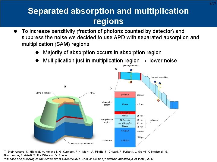
8/17 Separated absorption and multiplication regions To increase sensitivity (fraction of photons counted by detector) and suppress the noise we decided to use APD with separated absorption and multiplication (SAM) regions Majority of absorption occurs in absorption region Multiplication just in multiplication region → lower noise T. Steinhartova, C. Nichetti, M. Antonelli, G. Cautero, R. H. Menk, A. Pilotto, F. Driussi, P. Palestri, L. Selmi, K. Koshmak, S. Nannarone, F. Arfelli, S. Dal Zilio and G. Biasiol, Influence of δ p-doping on the behaviour of Ga. As/Al. Ga. As SAM-APDs for synchrotron radiation, J. of Instr. , 2017 8

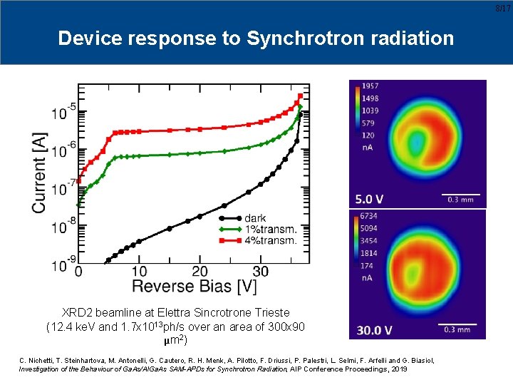
8/17 Device response to Synchrotron radiation XRD 2 beamline at Elettra Sincrotrone Trieste (12. 4 ke. V and 1. 7 x 10¹³ ph/s over an area of 300 x 90 μm 2) C. Nichetti, T. Steinhartova, M. Antonelli, G. Cautero, R. H. Menk, A. Pilotto, F. Driussi, P. Palestri, L. Selmi, F. Arfelli and G. Biasiol, Investigation of the Behaviour of Ga. As/Al. Ga. As SAM-APDs for Synchrotron Radiation, AIP Conference Proceedings, 2019

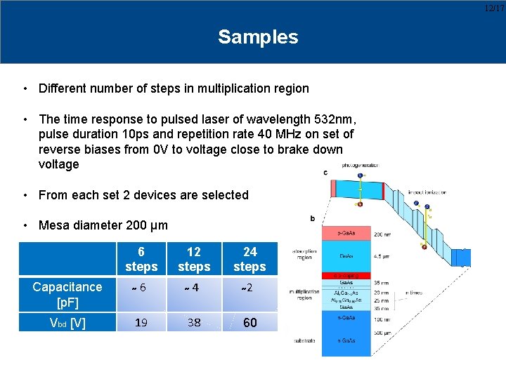
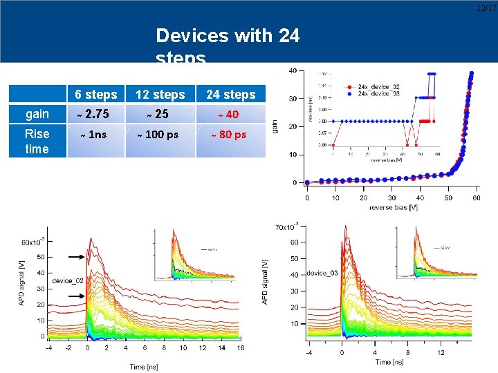
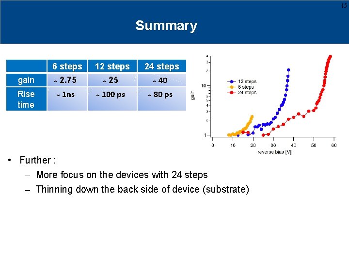
12/17 Samples • Different number of steps in multiplication region • The time response to pulsed laser of wavelength 532 nm, pulse duration 10 ps and repetition rate 40 MHz on set of reverse biases from 0 V to voltage close to brake down voltage • From each set 2 devices are selected • Mesa diameter 200 μm 6 steps 12 steps 24 steps Capacitance [p. F] 6 4 2 Vbd [V] 19 38 60

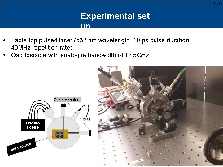
12/17 Experimental set up • Table-top pulsed laser (532 nm wavelength, 10 ps pulse duration, 40 MHz repetition rate) • Oscilloscope with analogue bandwidth of 12. 5 GHz Stepper motors Oscillo scope

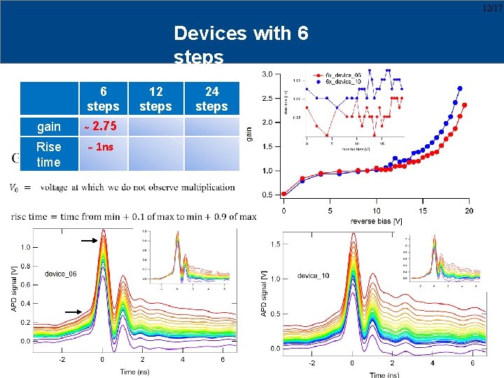
12/17 Devices with 6 steps gain 2. 75 Rise time 1 ns 12 steps 24 steps

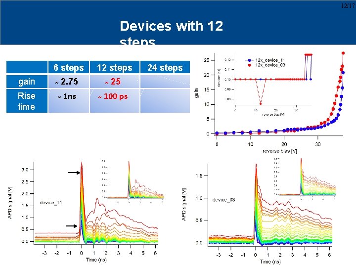
12/17 Devices with 12 steps 6 steps 12 steps gain 2. 75 25 Rise time 1 ns 100 ps 24 steps

12/17 Devices with 24 steps 6 steps 12 steps 24 steps gain 2. 75 25 40 Rise time 1 ns 100 ps 80 ps

15 Summary 6 steps 12 steps 24 steps gain 2. 75 25 40 Rise time 1 ns 100 ps 80 ps • Further : – More focus on the devices with 24 steps – Thinning down the back side of device (substrate)

17 Thanks to Giorgio Biasiol, C. Nichetti, M. Antonelli, R. H. Menk, F. Arfelli, G. Cautero, M. Danailov, S. dal Zilio SYRMEP, BEAR, SISSI, XRD 2 beamlines and Laser group at Elettra facility Dipartimento Politecnico di Ingegneria e Architettura - Università di Udine Università di Trieste funding: PRIN project 2015 WMZ 5 C 8 and to you for your attention!!