Operation of a silicon microstrip detector prototype for

- Slides: 1

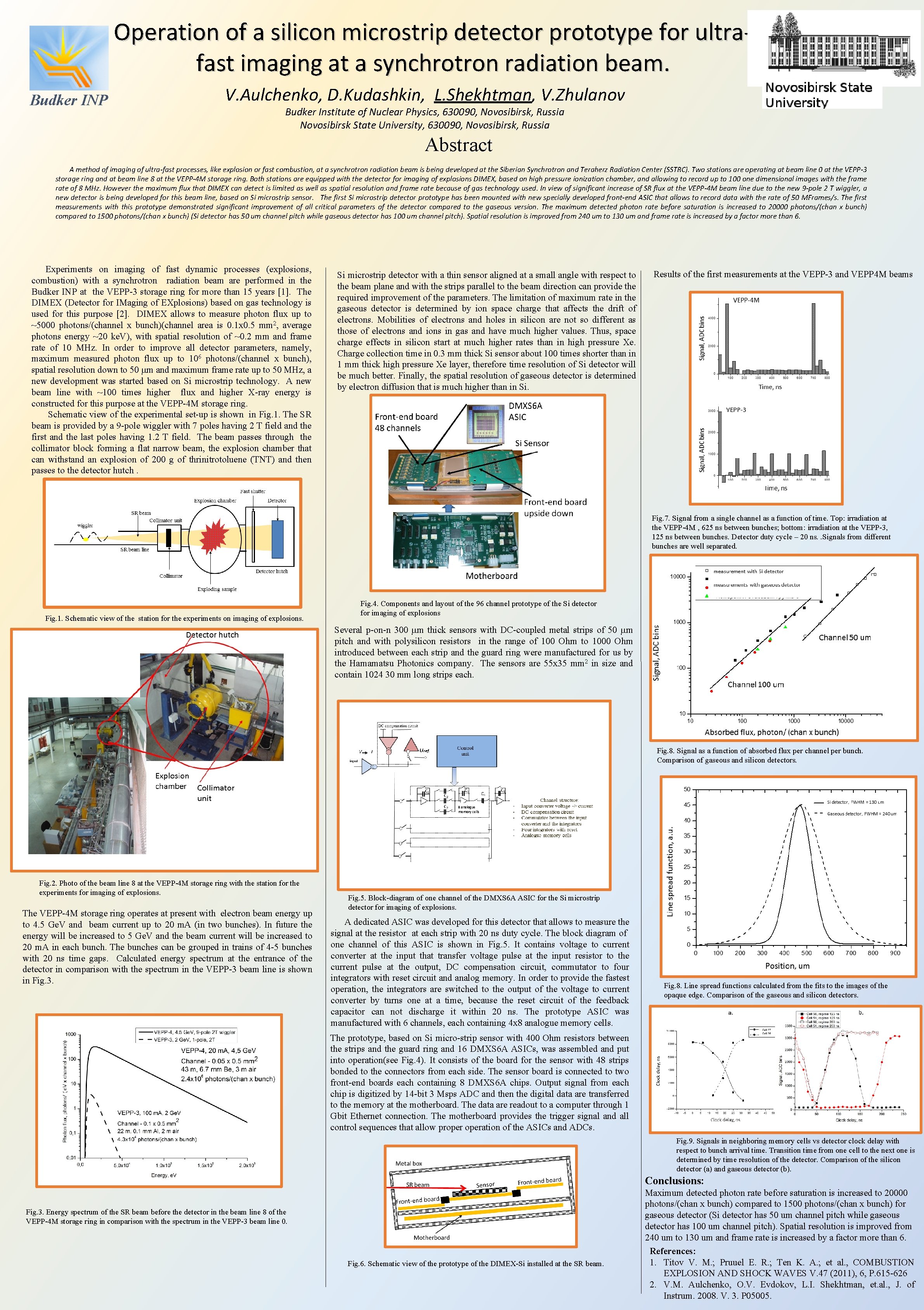
Operation of a silicon microstrip detector prototype for ultrafast imaging at a synchrotron radiation beam. Budker INP V. Aulchenko, D. Kudashkin, L. Shekhtman, V. Zhulanov Budker Institute of Nuclear Physics, 630090, Novosibirsk, Russia Novosibirsk State University, 630090, Novosibirsk, Russia Abstract A method of imaging of ultra-fast processes, like explosion or fast combustion, at a synchrotron radiation beam is being developed at the Siberian Synchrotron and Teraherz Radiation Center (SSTRC). Two stations are operating at beam line 0 at the VEPP-3 storage ring and at beam line 8 at the VEPP-4 M storage ring. Both stations are equipped with the detector for imaging of explosions DIMEX, based on high pressure ionization chamber, and allowing to record up to 100 one dimensional images with the frame rate of 8 MHz. However the maximum flux that DIMEX can detect is limited as well as spatial resolution and frame rate because of gas technology used. In view of significant increase of SR flux at the VEPP-4 M beam line due to the new 9 -pole 2 T wiggler, a new detector is being developed for this beam line, based on Si microstrip sensor. The first Si microstrip detector prototype has been mounted with new specially developed front-end ASIC that allows to record data with the rate of 50 MFrames/s. The first measurements with this prototype demonstrated significant improvement of all critical parameters of the detector compared to the gaseous version. The maximum detected photon rate before saturation is increased to 20000 photons/(chan x bunch) compared to 1500 photons/(chan x bunch) (Si detector has 50 um channel pitch while gaseous detector has 100 um channel pitch). Spatial resolution is improved from 240 um to 130 um and frame rate is increased by a factor more than 6. Experiments on imaging of fast dynamic processes (explosions, combustion) with a synchrotron radiation beam are performed in the Budker INP at the VEPP-3 storage ring for more than 15 years [1]. The DIMEX (Detector for IMaging of EXplosions) based on gas technology is used for this purpose [2]. DIMEX allows to measure photon flux up to ~5000 photons/(channel x bunch)(channel area is 0. 1 x 0. 5 mm 2, average photons energy ~20 ke. V), with spatial resolution of ~0. 2 mm and frame rate of 10 MHz. In order to improve all detector parameters, namely, maximum measured photon flux up to 106 photons/(channel x bunch), spatial resolution down to 50 mm and maximum frame rate up to 50 MHz, a new development was started based on Si microstrip technology. A new beam line with ~100 times higher flux and higher X-ray energy is constructed for this purpose at the VEPP-4 M storage ring. Schematic view of the experimental set-up is shown in Fig. 1. The SR beam is provided by a 9 -pole wiggler with 7 poles having 2 T field and the first and the last poles having 1. 2 T field. The beam passes through the collimator block forming a flat narrow beam, the explosion chamber that can withstand an explosion of 200 g of thrinitrotoluene (TNT) and then passes to the detector hutch. Si microstrip detector with a thin sensor aligned at a small angle with respect to the beam plane and with the strips parallel to the beam direction can provide the required improvement of the parameters. The limitation of maximum rate in the gaseous detector is determined by ion space charge that affects the drift of electrons. Mobilities of electrons and holes in silicon are not so different as those of electrons and ions in gas and have much higher values. Thus, space charge effects in silicon start at much higher rates than in high pressure Xe. Charge collection time in 0. 3 mm thick Si sensor about 100 times shorter than in 1 mm thick high pressure Xe layer, therefore time resolution of Si detector will be much better. Finally, the spatial resolution of gaseous detector is determined by electron diffusion that is much higher than in Si. Results of the first measurements at the VEPP-3 and VEPP 4 M beams Si Sensor Fig. 7. Signal from a single channel as a function of time. Top: irradiation at the VEPP-4 M , 625 ns between bunches; bottom: irradiation at the VEPP-3, 125 ns between bunches. Detector duty cycle – 20 ns. . Signals from different bunches are well separated. Fig. 1. Schematic view of the station for the experiments on imaging of explosions. Fig. 4. Components and layout of the 96 channel prototype of the Si detector for imaging of explosions Several p-on-n 300 mm thick sensors with DC-coupled metal strips of 50 mm pitch and with polysilicon resistors in the range of 100 Ohm to 1000 Ohm introduced between each strip and the guard ring were manufactured for us by the Hamamatsu Photonics company. The sensors are 55 x 35 mm 2 in size and contain 1024 30 mm long strips each. Fig. 8. Signal as a function of absorbed flux per channel per bunch. Comparison of gaseous and silicon detectors. 8 analogue memory cells Fig. 2. Photo of the beam line 8 at the VEPP-4 M storage ring with the station for the experiments for imaging of explosions. The VEPP-4 M storage ring operates at present with electron beam energy up to 4. 5 Ge. V and beam current up to 20 m. A (in two bunches). In future the energy will be increased to 5 Ge. V and the beam current will be increased to 20 m. A in each bunch. The bunches can be grouped in trains of 4 -5 bunches with 20 ns time gaps. Calculated energy spectrum at the entrance of the detector in comparison with the spectrum in the VEPP-3 beam line is shown in Fig. 3. Fig. 5. Block-diagram of one channel of the DMXS 6 A ASIC for the Si microstrip detector for imaging of explosions. A dedicated ASIC was developed for this detector that allows to measure the signal at the resistor at each strip with 20 ns duty cycle. The block diagram of one channel of this ASIC is shown in Fig. 5. It contains voltage to current converter at the input that transfer voltage pulse at the input resistor to the current pulse at the output, DC compensation circuit, commutator to four integrators with reset circuit and analog memory. In order to provide the fastest operation, the integrators are switched to the output of the voltage to current converter by turns one at a time, because the reset circuit of the feedback capacitor can not discharge it within 20 ns. The prototype ASIC was manufactured with 6 channels, each containing 4 x 8 analogue memory cells. Fig. 8. Line spread functions calculated from the fits to the images of the opaque edge. Comparison of the gaseous and silicon detectors. The prototype, based on Si micro-strip sensor with 400 Ohm resistors between the strips and the guard ring and 16 DMXS 6 A ASICs, was assembled and put into operation(see Fig. 4). It consists of the board for the sensor with 48 strips bonded to the connectors from each side. The sensor board is connected to two front-end boards each containing 8 DMXS 6 A chips. Output signal from each chip is digitized by 14 -bit 3 Msps ADC and then the digital data are transferred to the memory at the motherboard. The data are readout to a computer through 1 Gbit Ethernet connection. The motherboard provides the trigger signal and all control sequences that allow properation of the ASICs and ADCs. Fig. 9. Signals in neighboring memory cells vs detector clock delay with respect to bunch arrival time. Transition time from one cell to the next one is determined by time resolution of the detector. Comparison of the silicon detector (a) and gaseous detector (b). Conclusions: Fig. 3. Energy spectrum of the SR beam before the detector in the beam line 8 of the VEPP-4 M storage ring in comparison with the spectrum in the VEPP-3 beam line 0. Fig. 6. Schematic view of the prototype of the DIMEX-Si installed at the SR beam. Maximum detected photon rate before saturation is increased to 20000 photons/(chan x bunch) compared to 1500 photons/(chan x bunch) for gaseous detector (Si detector has 50 um channel pitch while gaseous detector has 100 um channel pitch). Spatial resolution is improved from 240 um to 130 um and frame rate is increased by a factor more than 6. References: 1. Titov V. M. ; Pruuel E. R. ; Ten K. A. ; et al. , COMBUSTION EXPLOSION AND SHOCK WAVES V. 47 (2011), 6, P. 615 -626 2. V. M. Aulchenko, O. V. Evdokov, L. I. Shekhtman, et. al. , J. of Instrum. 2008. V. 3. P 05005.