Master Colloquium Fieldeffect Control of Insulatormetal Transition Property

- Slides: 16
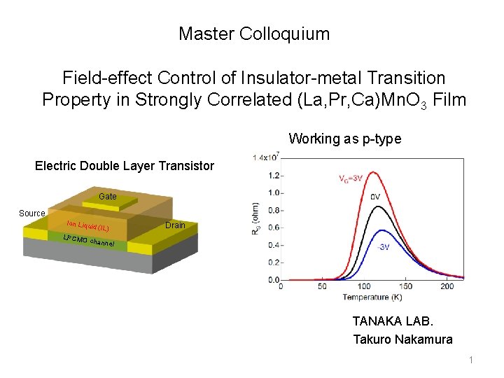
Master Colloquium Field-effect Control of Insulator-metal Transition Property in Strongly Correlated (La, Pr, Ca)Mn. O 3 Film Working as p-type Electric Double Layer Transistor Gate Source Ion Liqu Drain id (IL) LPCMO channe l TANAKA LAB. Takuro Nakamura 1
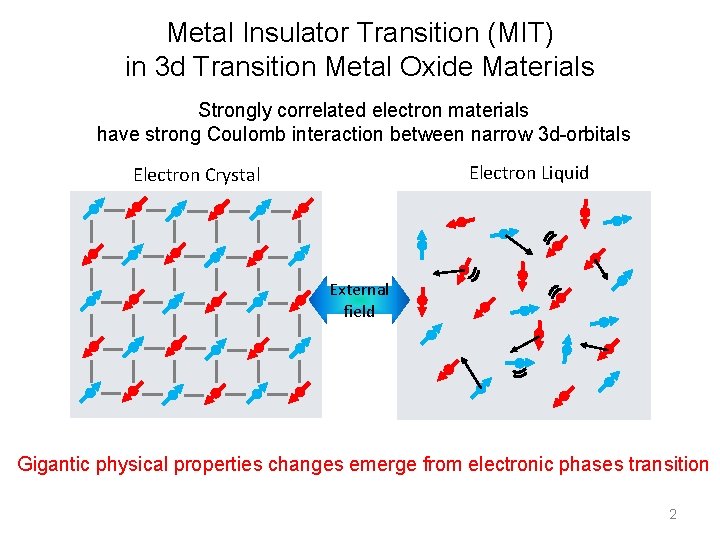
Metal Insulator Transition (MIT) in 3 d Transition Metal Oxide Materials Strongly correlated electron materials have strong Coulomb interaction between narrow 3 d-orbitals Electron Liquid Electron Crystal External field Gigantic physical properties changes emerge from electronic phases transition 2
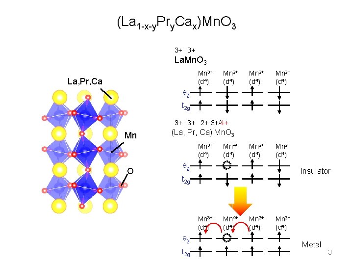
(La 1 -x-y. Pry. Cax)Mn. O 3 3+ 3+ La. Mn. O 3 Mn 3+ (d 4) La, Pr, Ca Mn 3+ (d 4) Mn 3+ (d 4) eg t 2 g 3+ 3+ 2+ 3+/4+ Mn (La, Pr, Ca) Mn. O 3 Mn 3+ (d 4) O Mn 4+ (d 4) eg Insulator t 2 g Mn 3+ (d 4) eg t 2 g Mn 4+ (d 4) Mn 3+ (d 4) Metal 3
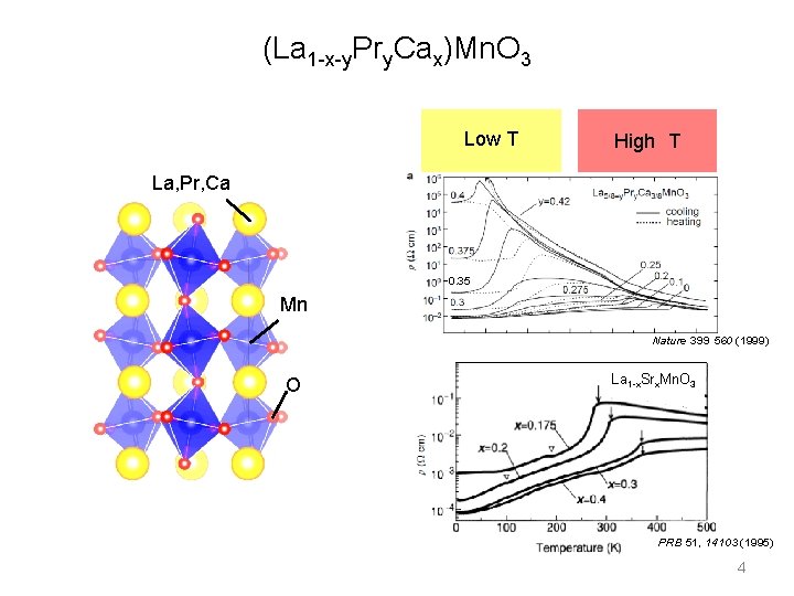
(La 1 -x-y. Pry. Cax)Mn. O 3 Low T High T La, Pr, Ca 0. 35 Mn Nature 399 560 (1999) O La 1 -x. Srx. Mn. O 3 PRB 51, 14103 (1995) 4
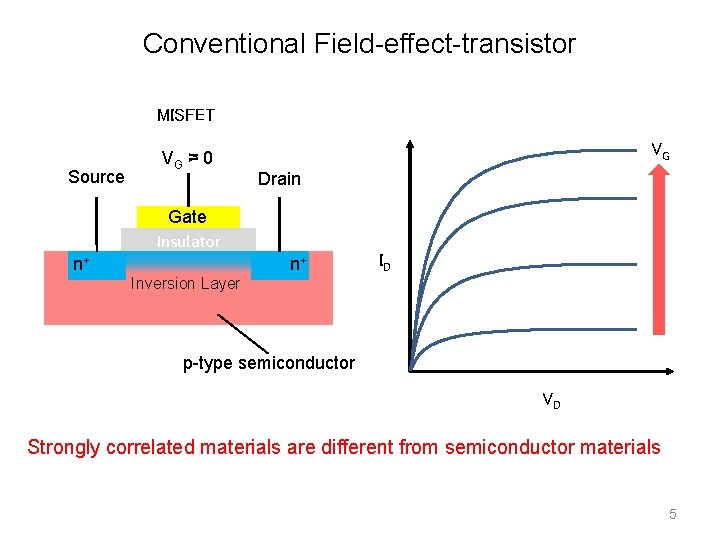
Conventional Field-effect-transistor MISFET Source VG > 0 = 0 VG Drain Gate Insulator n+ n+ ID Inversion Layer p-type semiconductor VD Strongly correlated materials are different from semiconductor materials 5
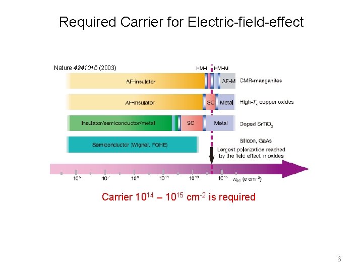
Required Carrier for Electric-field-effect Nature 4241015 (2003) Carrier 1014 – 1015 cm-2 is required 6
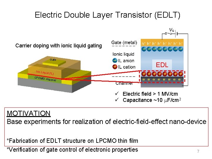
Electric Double Layer Transistor (EDLT) Carrier doping with ionic liquid gating Gate EDL Ion Liqu id (IL) LPCMO channe l ü Electric field > 1 MV/cm ü Capacitance ~10 m. F/cm 2 MOTIVATION Base experiments for realization of electric-field-effect nano-device *Fabrication of EDLT structure on LPCMO thin film *Verification of gate control of electronic properties 7
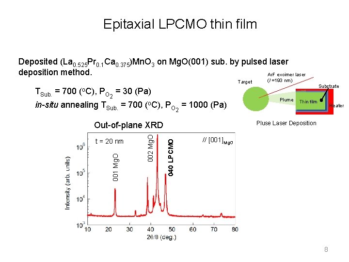
Epitaxial LPCMO thin film Deposited (La 0. 525 Pr 0. 1 Ca 0. 375)Mn. O 3 on Mg. O(001) sub. by pulsed laser deposition method. Ar. F excimer laser 040 LPCMO 002 Mg. O t = 20 nm Plume Substrate Thin film Heater Pluse Laser Deposition Out-of-plane XRD 001 Mg. O in-situ annealing TSub. = 700 (o. C), PO 2 = 1000 (Pa) (l =193 nm) TSub. = 700 (o. C), PO 2 = 30 (Pa) Target // [001]Mg. O 8
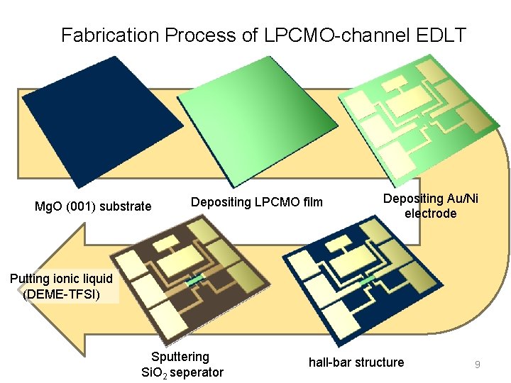
Fabrication Process of LPCMO-channel EDLT Mg. O (001) substrate Depositing LPCMO film Depositing Au/Ni electrode Putting ionic liquid (DEME-TFSI) Sputtering Si. O 2 seperator hall-bar structure 9
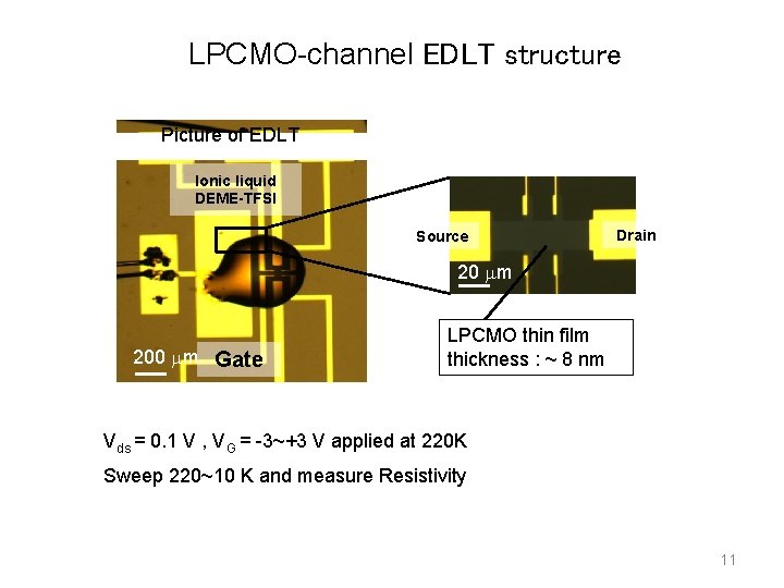
LPCMO-channel EDLT structure Picture of EDLT Ionic liquid DEME-TFSI Source Drain 20 mm 200 mm Gate LPCMO thin film thickness : ~ 8 nm Vds = 0. 1 V , VG = -3~+3 V applied at 220 K Sweep 220~10 K and measure Resistivity 11
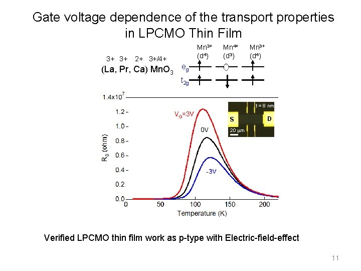
Gate voltage dependence of the transport properties in LPCMO Thin Film 3+ 3+ Mn 3+ (d 4) 2+ 3+/4+ Mn 4+ (d 3) Mn 3+ (d 4) (La, Pr, Ca) Mn. O 3 eg t 2 g t = 8 nm S D 20 mm Verified LPCMO thin film work as p-type with Electric-field-effect 11
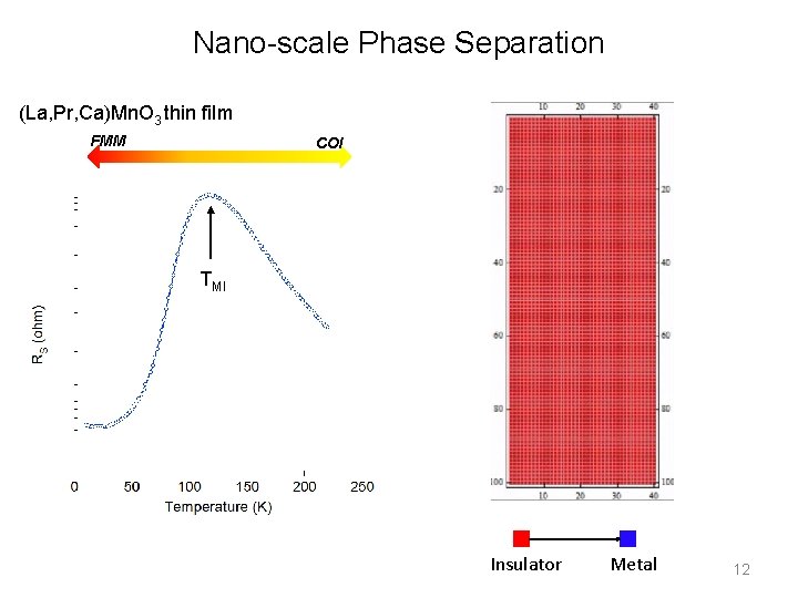
Nano-scale Phase Separation (La, Pr, Ca)Mn. O 3 thin film FMM COI TMI Insulator Metal 12
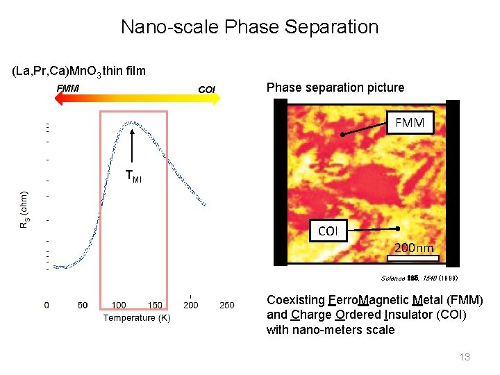
Nano-scale Phase Separation (La, Pr, Ca)Mn. O 3 thin film FMM COI Phase separation picture FMM TMI COI 200 nm Science 285, 1540 (1999) Coexisting Ferro. Magnetic Metal (FMM) and Charge Ordered Insulator (COI) with nano-meters scale 13
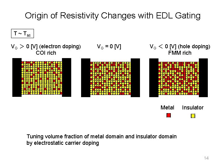
Origin of Resistivity Changes with EDL Gating T ~ TMI VG > 0 [V] (electron doping) COI rich VG = 0 [V] VG < 0 [V] (hole doping) FMM rich Metal Insulator Tuning volume fraction of metal domain and insulator domain by electrostatic carrier doping 14
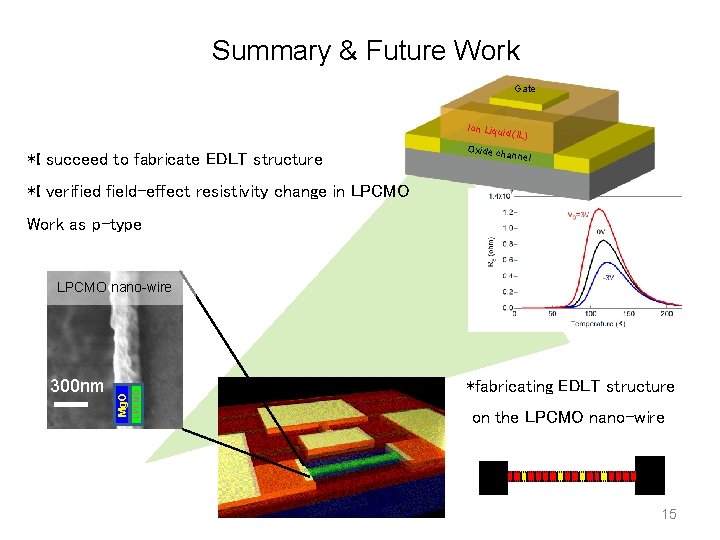
Summary & Future Work Gate *I succeed to fabricate EDLT structure Ion Liqu id (IL) Oxide ch annel *I verified field-effect resistivity change in LPCMO Work as p-type Mg. O 300 nm LPCMO nano-wire *fabricating EDLT structure on the LPCMO nano-wire 15
16