
LOGO 1990 70 2000 50 30 2010 32


- Slides: 18
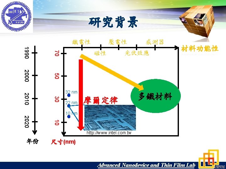
LOGO 研究背景 鐵電性 壓電性 1990 70 2000 50 磁性 光伏效應 30 2010 32 nm 22 nm 感測器 摩爾定律 材料功能性 多鐵材料 10 2020 10 nm http: //www. intel. com. tw 年份 尺寸(nm) Advanced Nanodevice and Thin Film Lab
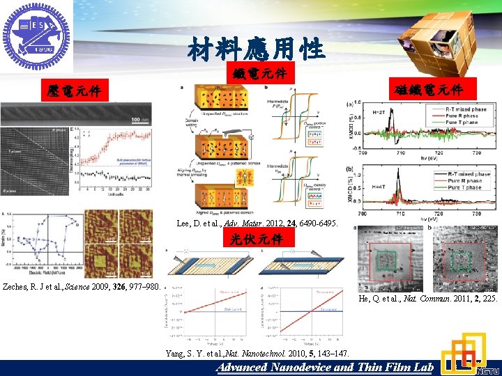
LOGO 材料應用性 鐵電元件 磁鐵電元件 壓電元件 Lee, D. et al. , Adv. Mater. 2012, 24, 6490 -6495. 光伏元件 Zeches, R. J et al. , Science 2009, 326, 977– 980. He, Q. et al. , Nat. Commun. 2011, 2, 225. Yang, S. Y. et al. , Nat. Nanotechnol. 2010, 5, 143– 147. Advanced Nanodevice and Thin Film Lab
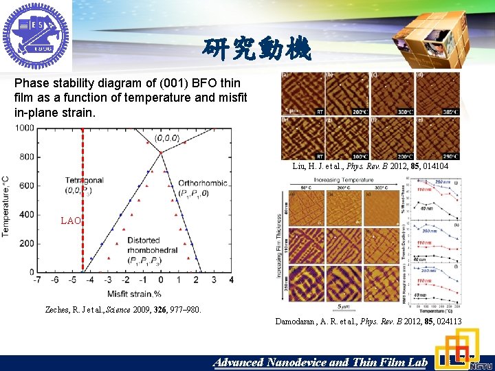
LOGO 研究動機 Phase stability diagram of (001) BFO thin film as a function of temperature and misfit in-plane strain. Liu, H. J. et al. , Phys. Rev. B 2012, 85, 014104 LAO Zeches, R. J et al. , Science 2009, 326, 977– 980. Damodaran , A. R. et al. , Phys. Rev. B 2012, 85, 024113 Advanced Nanodevice and Thin Film Lab
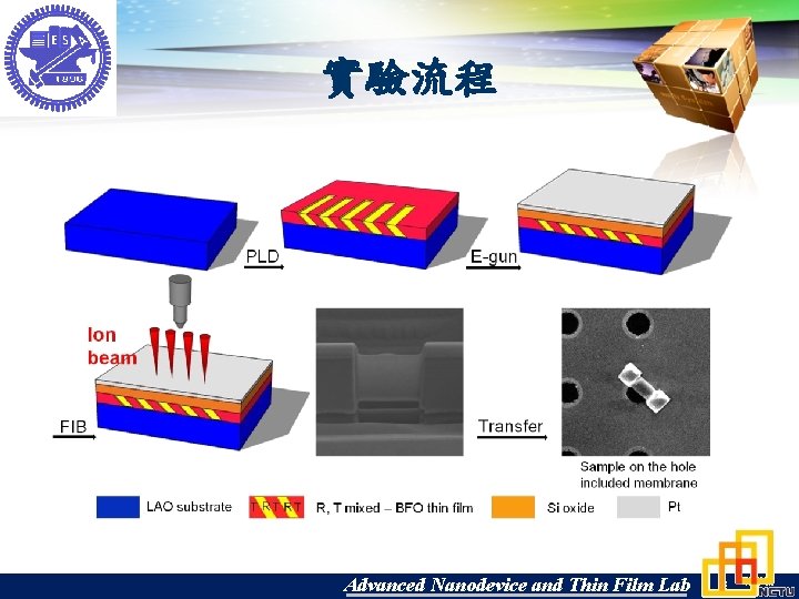
LOGO 實驗流程 Advanced Nanodevice and Thin Film Lab
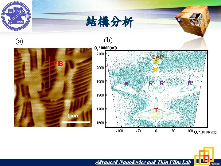
LOGO 結構分析 (b) (a) Qy*10000(url) 2100 FIB LAO 2000 R 1900 R’ R’ 1800 T 1700 1μm 1600 -100 -50 0 50 100 Q *10000(url) x Advanced Nanodevice and Thin Film Lab
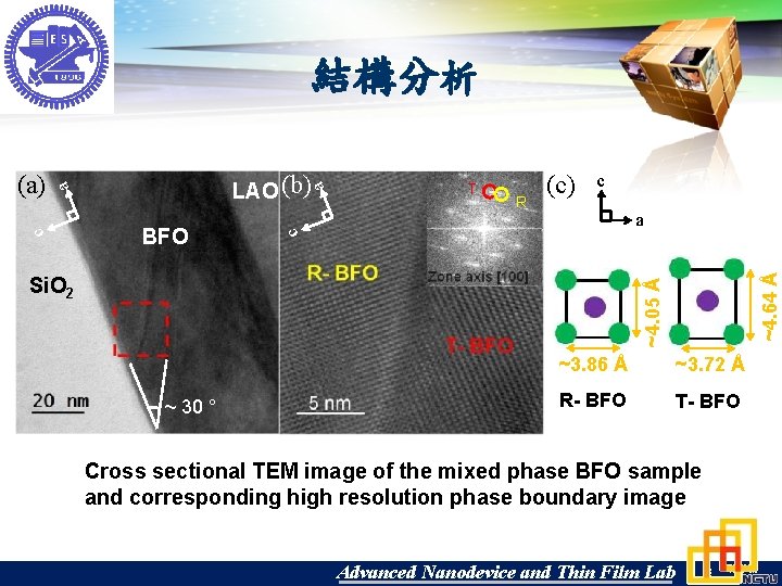
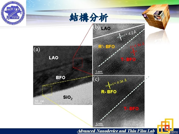
LOGO 結構分析 R a (c) c a c BFO T ~4. 05 Å Si. O 2 ~4. 64 Å LAO (b) a c (a) ~ 30 ° ~3. 86 Å ~3. 72 Å R- BFO T- BFO Cross sectional TEM image of the mixed phase BFO sample and corresponding high resolution phase boundary image Advanced Nanodevice and Thin Film Lab
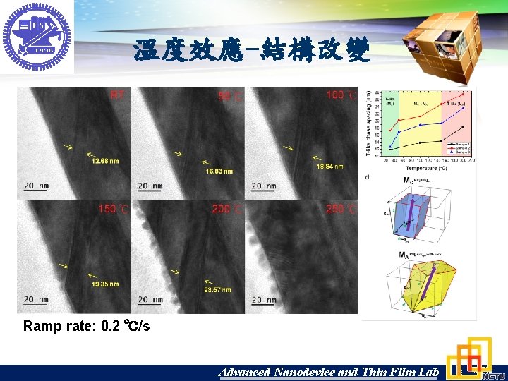
LOGO 溫度效應-結構改變 Ramp rate: 0. 2 ℃/s Advanced Nanodevice and Thin Film Lab
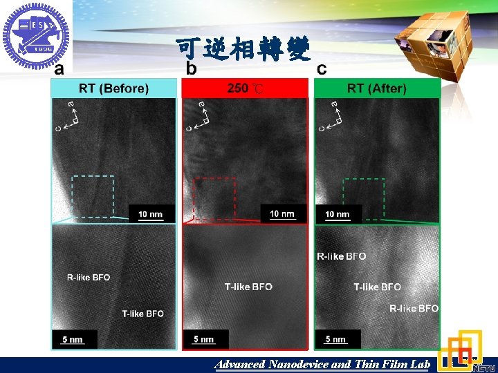
LOGO 可逆相轉變 (c) (d) Advanced Nanodevice and Thin Film Lab
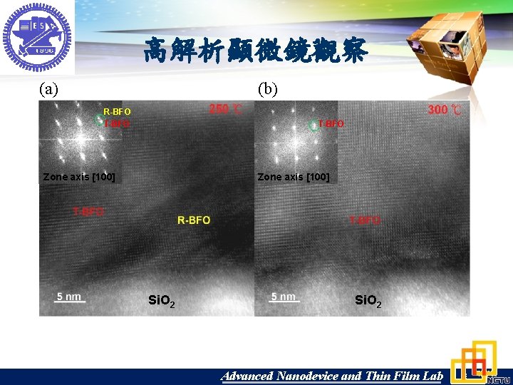
LOGO 高解析顯微鏡觀察 (a) (b) R-BFO T-BFO Zone axis [100] Si. O 2 Advanced Nanodevice and Thin Film Lab
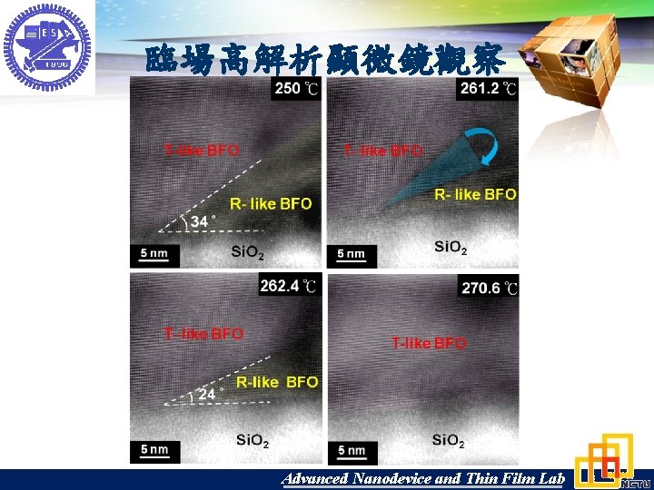
LOGO 臨場高解析顯微鏡觀察 Advanced Nanodevice and Thin Film Lab
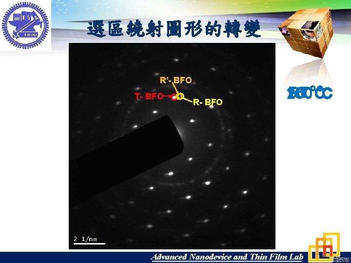
LOGO 選區繞射圖形的轉變 R’- BFO T- BFO RT 150 50 ℃ ℃ 200 Advanced Nanodevice and Thin Film Lab
LOGO 結構分析 (b)(b) LAO (a) 2Å c= 4. 4Å c= 4. 6 R’- BFO LAO T- BFO (c) 4Å 0 c= 4. R- BFO Si. O 2 T- BFO Advanced Nanodevice and Thin Film Lab
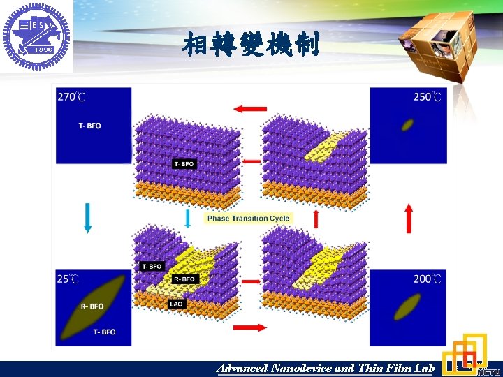
LOGO 相轉變機制 Advanced Nanodevice and Thin Film Lab
LOGO 結論 v BFO thin film exhibited R→T phase transition with increasing temperature. Upon increasing the temperature from room temperature to 200℃, we found a significant increase in the width of T-phase region with the broader morphology phase boundary (MPB). v Upon further increasing the temperature, the MPB disappears gradually with the change of tilt angle that probably attribute to the emergence of intermediate R’- phase. Eventually, only T-phase BFO would be preserved at high temperature. v The mixed-phase stripes with fringes are found to recover upon cooling back to room temperature although they don’t exactly appear at the same locations. Advanced Nanodevice and Thin Film Lab
LOGO Thanks for your attention Advanced Nanodevice and Thin Film Lab