Lecture 14 OUTLINE pn junction electrostatics Reading Chapter
- Slides: 13

Lecture #14 OUTLINE • pn junction electrostatics Reading: Chapter 5 Spring 2007 EE 130 Lecture 14, Slide 1

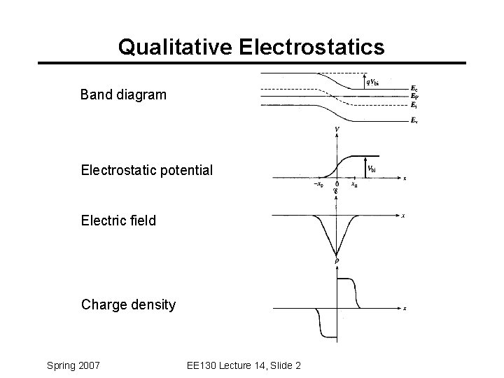
Qualitative Electrostatics Band diagram Electrostatic potential Electric field Charge density Spring 2007 EE 130 Lecture 14, Slide 2

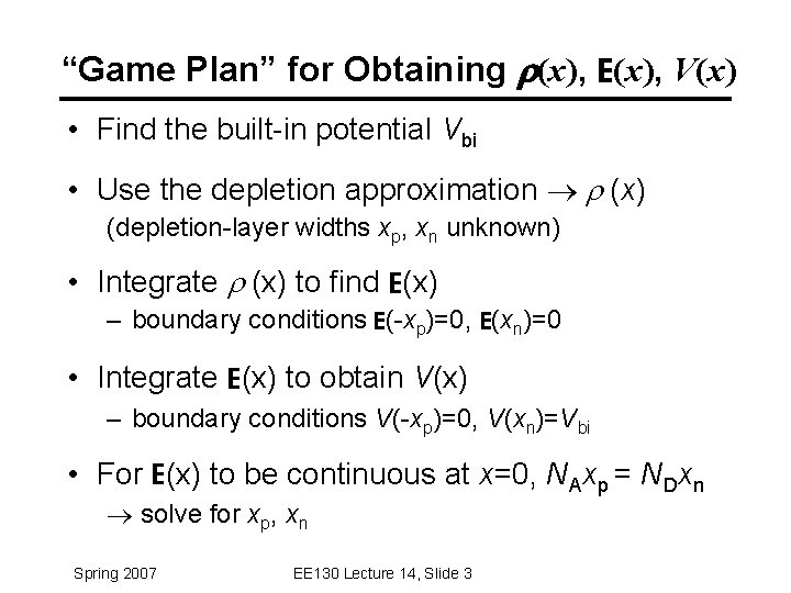
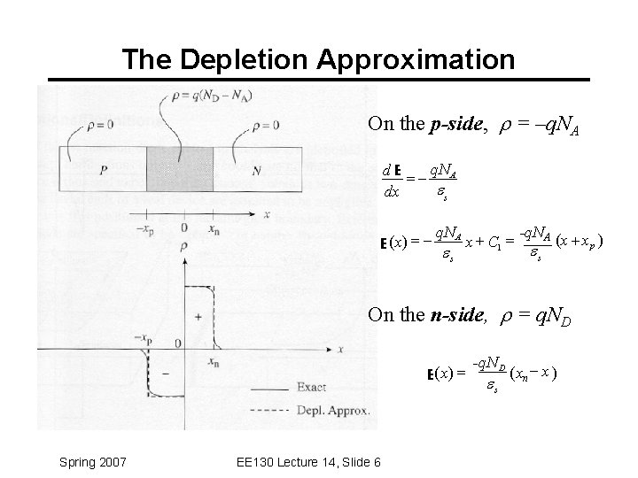
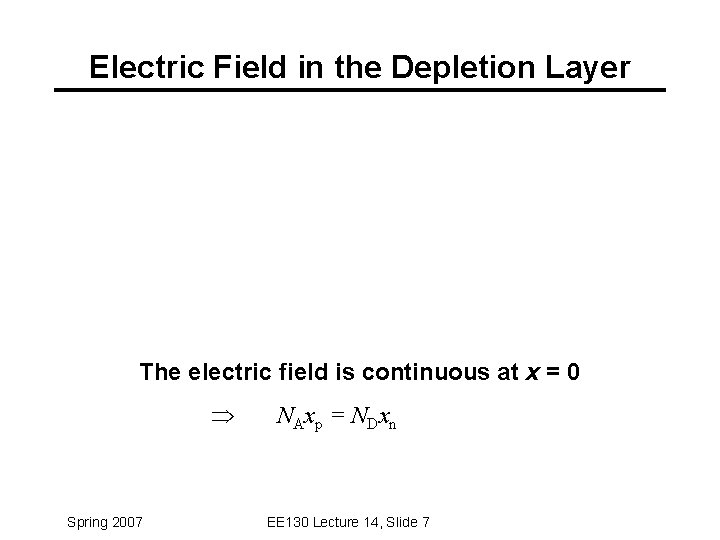
“Game Plan” for Obtaining r(x), E(x), V(x) • Find the built-in potential Vbi • Use the depletion approximation (x) (depletion-layer widths xp, xn unknown) • Integrate (x) to find E(x) – boundary conditions E(-xp)=0, E(xn)=0 • Integrate E(x) to obtain V(x) – boundary conditions V(-xp)=0, V(xn)=Vbi • For E(x) to be continuous at x=0, NAxp = NDxn solve for xp, xn Spring 2007 EE 130 Lecture 14, Slide 3

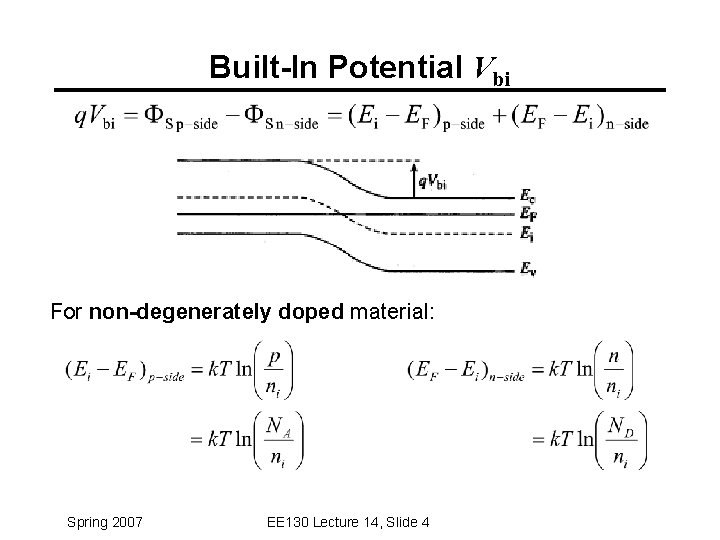
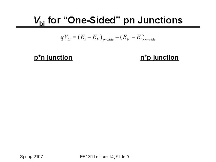
Built-In Potential Vbi For non-degenerately doped material: Spring 2007 EE 130 Lecture 14, Slide 4

Vbi for “One-Sided” pn Junctions p+n junction Spring 2007 n+p junction EE 130 Lecture 14, Slide 5

The Depletion Approximation On the p-side, = –q. NA q. N d. E =- A es dx E ( x) = - q. N A es x + C 1 = -q. NA es (x + x p ) On the n-side, = q. ND E ( x) = Spring 2007 EE 130 Lecture 14, Slide 6 -q. N D es ( xn - x )

Electric Field in the Depletion Layer The electric field is continuous at x = 0 Spring 2007 N Ax p = N Dx n EE 130 Lecture 14, Slide 7

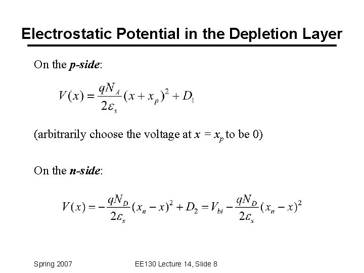
Electrostatic Potential in the Depletion Layer On the p-side: (arbitrarily choose the voltage at x = xp to be 0) On the n-side: Spring 2007 EE 130 Lecture 14, Slide 8

• At x = 0, expressions for p-side and n-side must be equal: • We also know that NAxp = NDxn Spring 2007 EE 130 Lecture 14, Slide 9

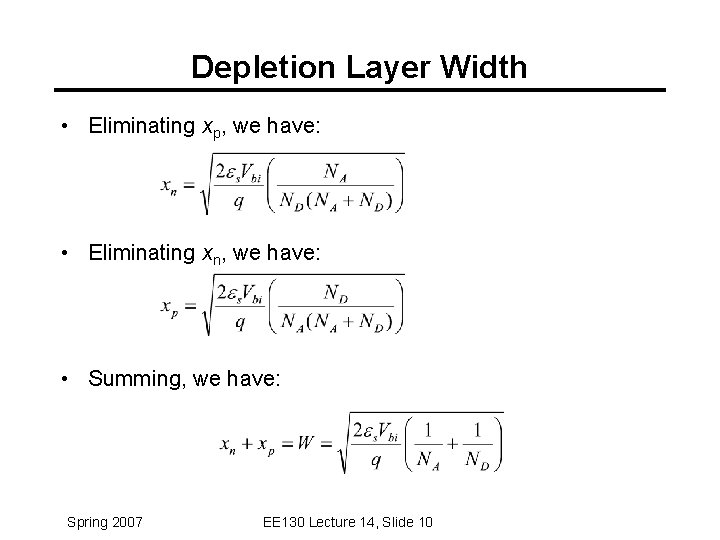
Depletion Layer Width • Eliminating xp, we have: • Eliminating xn, we have: • Summing, we have: Spring 2007 EE 130 Lecture 14, Slide 10

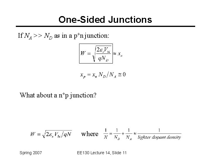
One-Sided Junctions If NA >> ND as in a p+n junction: What about a n+p junction? where Spring 2007 EE 130 Lecture 14, Slide 11

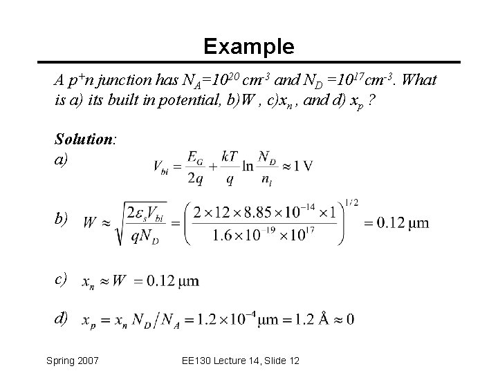
Example A p+n junction has NA=1020 cm-3 and ND =1017 cm-3. What is a) its built in potential, b)W , c)xn , and d) xp ? Solution: a) b) c) d) Spring 2007 EE 130 Lecture 14, Slide 12

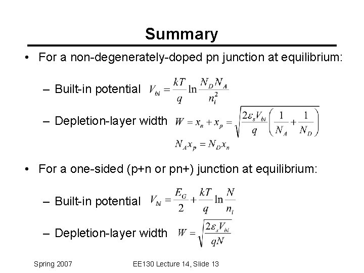
Summary • For a non-degenerately-doped pn junction at equilibrium: – Built-in potential – Depletion-layer width • For a one-sided (p+n or pn+) junction at equilibrium: – Built-in potential – Depletion-layer width Spring 2007 EE 130 Lecture 14, Slide 13