Interconnect Technologies and Drivers primary technologies integration optics
- Slides: 6

Interconnect Technologies and Drivers • primary technologies: integration + optics • driven primarily by servers/cloud computing • thin wires → slow wires; limits ability to scale interconnect • higher core count → less I/O bandwidth per core • space/power reduction likely to drive if power+thermal challenges overcome • challenges • process cost and maturity • component lifetime • coupled time scales for processor+network • some commoditization from home networking?

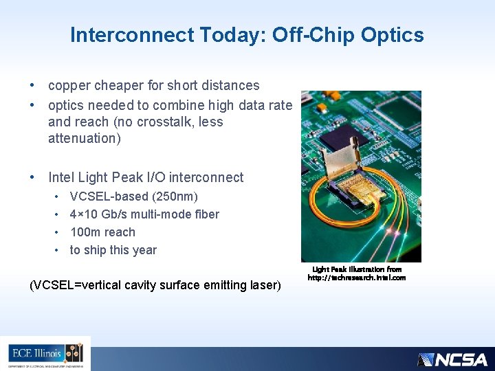
Interconnect Today: Off-Chip Optics • copper cheaper for short distances • optics needed to combine high data rate and reach (no crosstalk, less attenuation) • Intel Light Peak I/O interconnect • • VCSEL-based (250 nm) 4× 10 Gb/s multi-mode fiber 100 m reach to ship this year (VCSEL=vertical cavity surface emitting laser) Light Peak illustration from http: //techresearch. intel. com

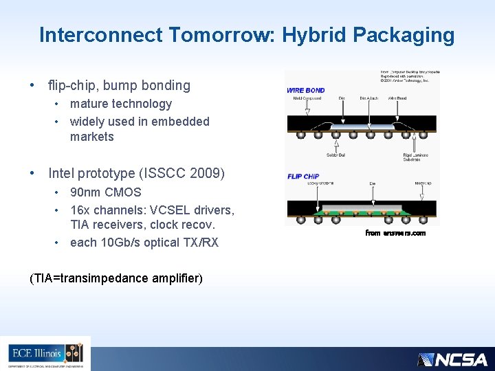
Interconnect Tomorrow: Hybrid Packaging • flip-chip, bump bonding • mature technology • widely used in embedded markets • Intel prototype (ISSCC 2009) • 90 nm CMOS • 16 x channels: VCSEL drivers, TIA receivers, clock recov. • each 10 Gb/s optical TX/RX (TIA=transimpedance amplifier) from answers. com

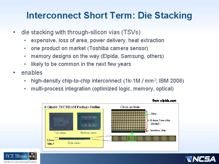
Interconnect Short Term: Die Stacking • die stacking with through-silicon vias (TSVs) • • expensive, loss of area, power delivery, heat extraction one product on market (Toshiba camera sensor) memory designs on the way (Elpida, Samsung, others) likely to be common in the next few years • enables • high-density chip-to-chip interconnect (1 k-1 M / mm 2; IBM 2008) • multi-process integration (optimized logic, memory, optical) from elpida. com

Chip-to-Chip Optics Examples • several companies developing • Intel: ISSCC Feb 2009 • IBM Research roadmap • next 5 years on card • later for Multi-chip Modules • Hewlett-Packard • architectural elements • IBM 160 Gb/s printed circuit board optical bus (2008) • Hewlett-Packard • board to board free space optics at 240 Gb/s (2008) • optical multidrop bus (2009)

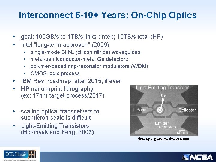
Interconnect 5 -10+ Years: On-Chip Optics • goal: 100 GB/s to 1 TB/s links (Intel); 10 TB/s total (HP) • Intel “long-term approach” (2009) • • single-mode Si 3 N 4 (silicon nitride) waveguides metal-semiconductor-metal Ge detectors polymer-based ring-resonator modulators (WDM) CMOS logic process • IBM Res. roadmap: after 2015, if ever • HP nanoimprint lithography (ex: 17 nm target process/2017) • scaling optical transceivers to submicron scale is difficult • Light-Emitting Transistors (Holonyak and Feng, 2003) from aip. org (source Physics News)