Influence of Tin Doped Cadmium Oxide on Structural

- Slides: 1

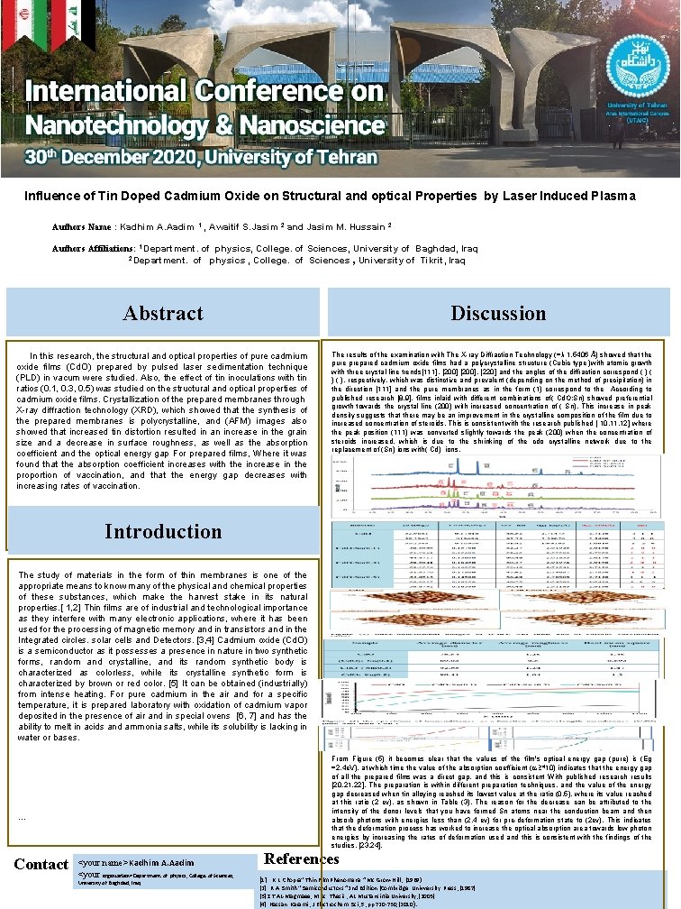
Influence of Tin Doped Cadmium Oxide on Structural and optical Properties by Laser Induced Plasma Authors Name : Kadhim A. Aadim 1 , Awaitif S. Jasim 2 and Jasim M. Hussain 2 Authors Affiliations: 1 Department. of physics, College. of Sciences, University of Baghdad, Iraq 2 Department. of physics , College. of Sciences , University of Tikrit, Iraq Abstract Discussion In this research, the structural and optical properties of pure cadmium oxide films (Cd. O) prepared by pulsed laser sedimentation technique (PLD) in vacum were studied. Also, the effect of tin inoculations with tin ratios (0. 1, 0. 3, 0. 5) was studied on the structural and optical properties of cadmium oxide films. Crystallization of the prepared membranes through X-ray diffraction technology (XRD), which showed that the synthesis of the prepared membranes is polycrystalline, and (AFM) images also showed that increased tin distortion resulted in an increase in the grain size and a decrease in surface roughness, as well as the absorption coefficient and the optical energy gap For prepared films, Where it was found that the absorption coefficient increases with the increase in the proportion of vaccination, and that the energy gap decreases with increasing rates of vaccination. … The results of the examination with The X-ray Diffraction Technology (=λ 1. 5406 Å) showed that the pure prepared cadmium oxide films had a polycrystalline structure (Cubic type )with atomic growth with three crystal line trends[111], [200], [220] and the angles of the diffraction correspond ( ) ( ), respectively, which was distinctive and prevalent (depending on the method of precipitation) in the direction [111] and the pure membranes as in the form (1) correspond to the According to published research [8, 9], films inlaid with different combinations of( Cd. O: Sn) showed preferential growth towards the crystal line (200) with increased concentration of ( Sn). This increase in peak density suggests that there may be an improvement in the crystalline composition of the film due to increased concentration of steroids. This is consistent with the research published [ 10, 11, 12] where the peak position (111) was converted slightly towards the peak (200) when the concentration of steroids increased, which is due to the shrinking of the cdo crystalline network due to the replacement of (Sn) ions with( Cd) ions. Introduction The study of materials in the form of thin membranes is one of the appropriate means to know many of the physical and chemical properties of these substances, which make the harvest stake in its natural properties. [ 1, 2] Thin films are of industrial and technological importance as they interfere with many electronic applications, where it has been used for the processing of magnetic memory and in transistors and in the Integrated circles. solar cells and Detectors. [3, 4] Cadmium oxide (Cd. O) is a semiconductor as it possesses a presence in nature in two synthetic forms, random and crystalline, and its random synthetic body is characterized as colorless, while its crystalline synthetic form is characterized by brown or red color. [5] It can be obtained (industrially) from intense heating. For pure cadmium in the air and for a specific temperature, it is prepared laboratory with oxidation of cadmium vapor deposited in the presence of air and in special ovens [6, 7] and has the ability to melt in acids and ammonia salts, while its solubility is lacking in water or bases. From Figure (5) it becomes clear that the values of the film's optical energy gap (pure) is (Eg =2. 4 e. V), at which time the value of the absorption coefficient ( 410) indicates that the energy gap of all the prepared films was a direct gap, and this is consistent With published research results [20, 21, 22]. The preparation is within different preparation techniques, and the value of the energy gap decreased when tin alloying reached its lowest value at the ratio (0. 5), where its value reached at this ratio (2 ev), as shown in Table (3). The reason for the decrease can be attributed to the intensity of the donor levels that you have formed Sn atoms near the conduction beam and then absorb photons with energies less than (2. 4 ev) for pre-deformation state to (2 ev). This indicates that the deformation process has worked to increase the optical absorption area towards low photon energies by increasing the rates of deformation used and this is consistent with the findings of the studies. [23, 24]. … Contact <your name>Kadhim A. Aadim <your organization>Department. of physics, College. of Sciences, University of Baghdad, Iraq References [1] K. L. Chopra“ Thin Film Phenomena ” Mc Grow-Hill , (1969). [2] R. A. Smith “ Semiconductors ” 2 nd Edition (Combridge Univversity Press , (1987). [3] Z. T. AL-Magmaee, M. Sc. Thesis , AL Mustansirtia University, (2003). [4] Hassan Karami , J. Electrochem. Sci. , 5 , pp 720 -730, (2010 ).