EECS 40 Spring 2003 Lecture 21 S Ross
- Slides: 16

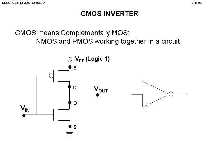
EECS 40 Spring 2003 Lecture 21 S. Ross CMOS INVERTER CMOS means Complementary MOS: NMOS and PMOS working together in a circuit VDD (Logic 1) S D VIN D S VOUT

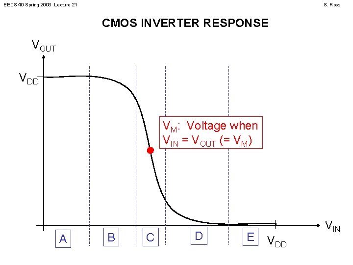
EECS 40 Spring 2003 Lecture 21 S. Ross CMOS INVERTER RESPONSE VOUT VDD VM: Voltage when VIN = VOUT (= VM) A B C D E VIN VDD

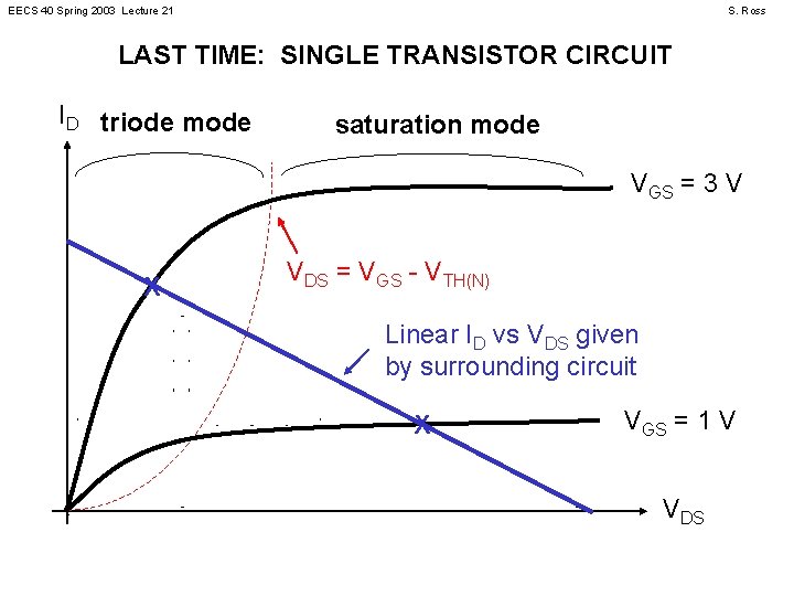
EECS 40 Spring 2003 Lecture 21 S. Ross LAST TIME: SINGLE TRANSISTOR CIRCUIT ID triode mode saturation mode VGS = 3 V X VDS = VGS - VTH(N) Linear ID vs VDS given by surrounding circuit X VGS = 1 V VDS

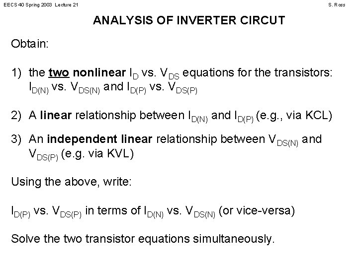
EECS 40 Spring 2003 Lecture 21 S. Ross ANALYSIS OF INVERTER CIRCUT Obtain: 1) the two nonlinear ID vs. VDS equations for the transistors: ID(N) vs. VDS(N) and ID(P) vs. VDS(P) 2) A linear relationship between ID(N) and ID(P) (e. g. , via KCL) 3) An independent linear relationship between VDS(N) and VDS(P) (e. g. via KVL) Using the above, write: ID(P) vs. VDS(P) in terms of ID(N) vs. VDS(N) (or vice-versa) Solve the two transistor equations simultaneously.

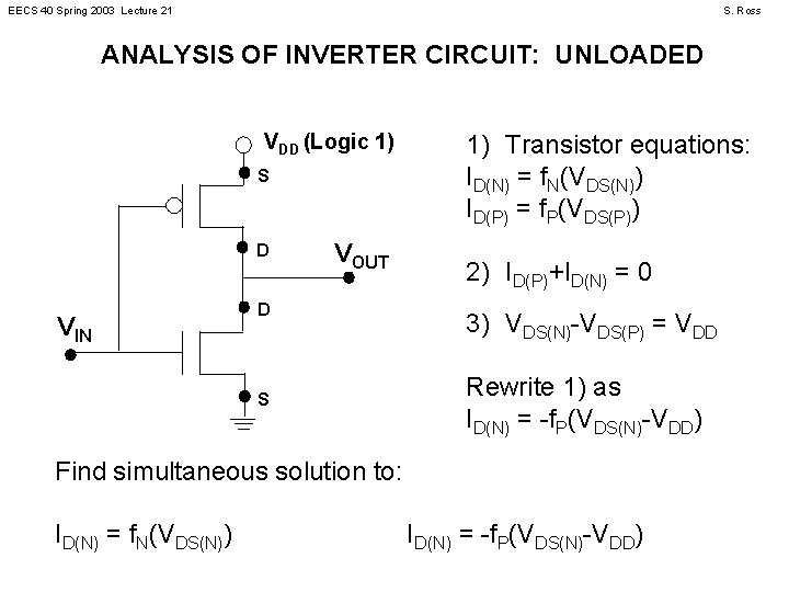
EECS 40 Spring 2003 Lecture 21 S. Ross ANALYSIS OF INVERTER CIRCUIT: UNLOADED VDD (Logic 1) S D VIN VOUT D S 1) Transistor equations: ID(N) = f. N(VDS(N)) ID(P) = f. P(VDS(P)) 2) ID(P)+ID(N) = 0 3) VDS(N)-VDS(P) = VDD Rewrite 1) as ID(N) = -f. P(VDS(N)-VDD) Find simultaneous solution to: ID(N) = f. N(VDS(N)) ID(N) = -f. P(VDS(N)-VDD)

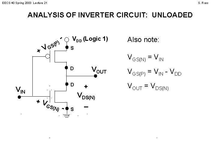
EECS 40 Spring 2003 Lecture 21 S. Ross ANALYSIS OF INVERTER CIRCUIT: UNLOADED (P) - GS V + VDD (Logic 1) Also note: S VGS(N) = VIN VOUT D D VIN +V GS(N ) - S + VDS(N) _ VGS(P) = VIN - VDD VOUT = VDS(N)

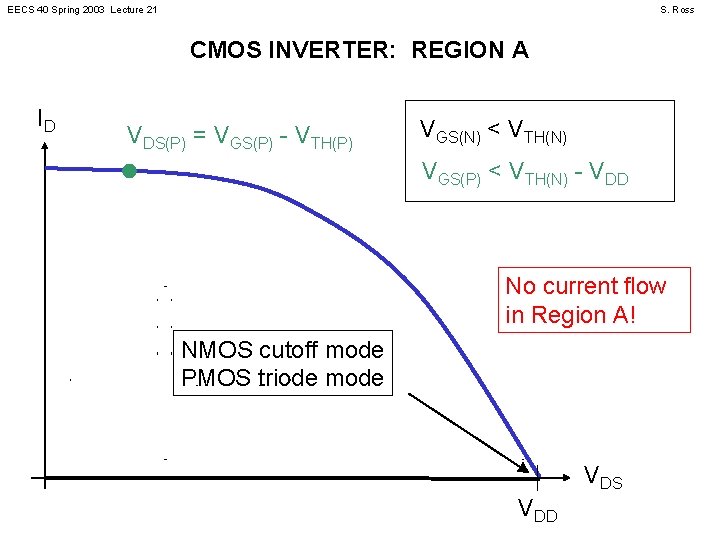
EECS 40 Spring 2003 Lecture 21 S. Ross CMOS INVERTER: REGION A ID VDS(P) = VGS(P) - VTH(P) VGS(N) < VTH(N) VGS(P) < VTH(N) - VDD No current flow in Region A! NMOS cutoff mode PMOS triode mode VDS VDD

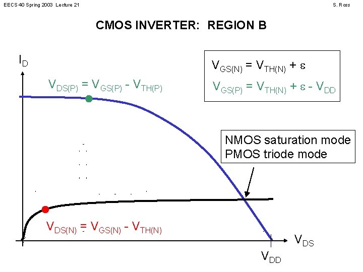
EECS 40 Spring 2003 Lecture 21 S. Ross CMOS INVERTER: REGION B ID VGS(N) = VTH(N) + e VDS(P) = VGS(P) - VTH(P) VGS(P) = VTH(N) + e - VDD NMOS saturation mode PMOS triode mode VDS(N) = VGS(N) - VTH(N) VDS VDD

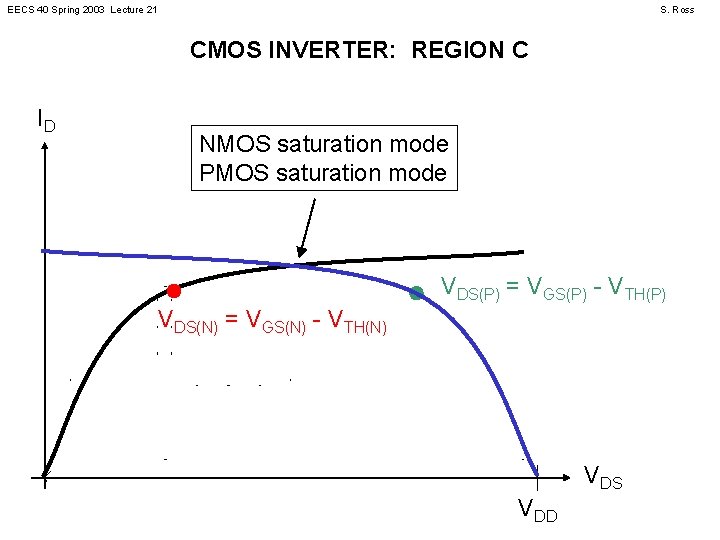
EECS 40 Spring 2003 Lecture 21 S. Ross CMOS INVERTER: REGION C ID NMOS saturation mode PMOS saturation mode VDS(P) = VGS(P) - VTH(P) VDS(N) = VGS(N) - VTH(N) VDS VDD

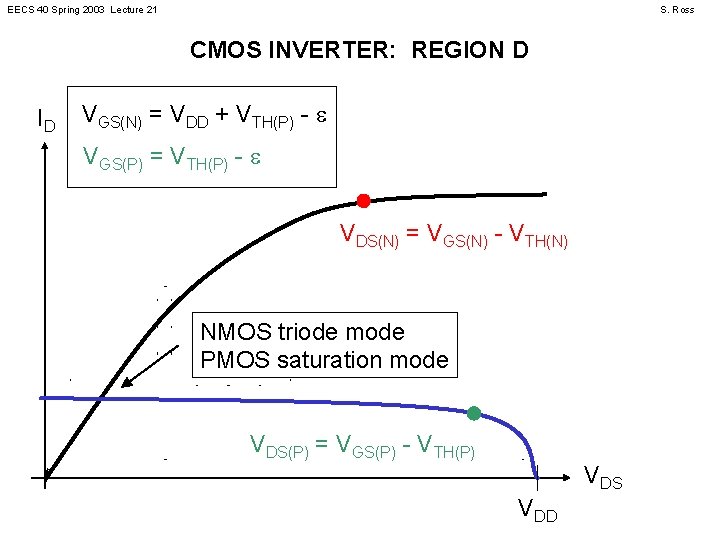
EECS 40 Spring 2003 Lecture 21 S. Ross CMOS INVERTER: REGION D ID VGS(N) = VDD + VTH(P) - e VGS(P) = VTH(P) - e VDS(N) = VGS(N) - VTH(N) NMOS triode mode PMOS saturation mode VDS(P) = VGS(P) - VTH(P) VDS VDD

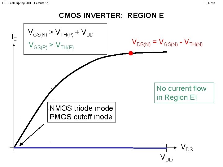
EECS 40 Spring 2003 Lecture 21 S. Ross CMOS INVERTER: REGION E ID VGS(N) > VTH(P) + VDD VGS(P) > VTH(P) VDS(N) = VGS(N) - VTH(N) No current flow in Region E! NMOS triode mode PMOS cutoff mode VDS VDD

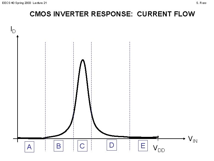
EECS 40 Spring 2003 Lecture 21 S. Ross CMOS INVERTER RESPONSE: CURRENT FLOW ID A B C D E VIN VDD

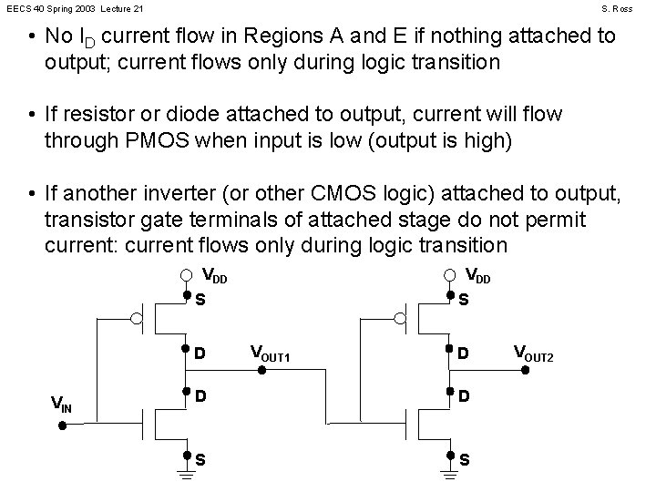
EECS 40 Spring 2003 Lecture 21 S. Ross • No ID current flow in Regions A and E if nothing attached to output; current flows only during logic transition • If resistor or diode attached to output, current will flow through PMOS when input is low (output is high) • If another inverter (or other CMOS logic) attached to output, transistor gate terminals of attached stage do not permit current: current flows only during logic transition VDD S D VIN S VOUT 1 D D D S S VOUT 2

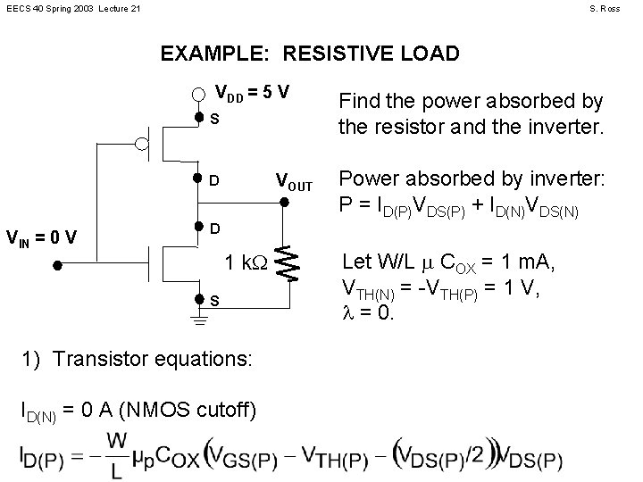
EECS 40 Spring 2003 Lecture 21 S. Ross EXAMPLE: RESISTIVE LOAD VDD = 5 V S VOUT D VIN = 0 V Find the power absorbed by the resistor and the inverter. Power absorbed by inverter: P = ID(P)VDS(P) + ID(N)VDS(N) D 1 k. W S 1) Transistor equations: ID(N) = 0 A (NMOS cutoff) Let W/L m COX = 1 m. A, VTH(N) = -VTH(P) = 1 V, l = 0.

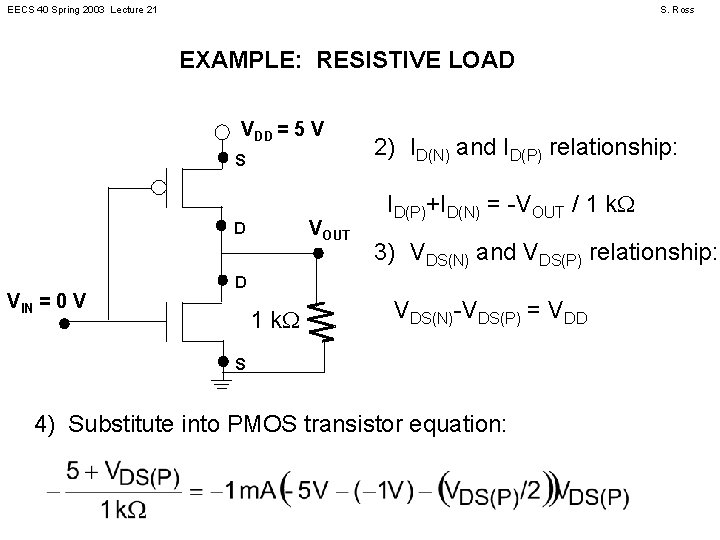
EECS 40 Spring 2003 Lecture 21 S. Ross EXAMPLE: RESISTIVE LOAD VDD = 5 V S VOUT D VIN = 0 V 2) ID(N) and ID(P) relationship: ID(P)+ID(N) = -VOUT / 1 k. W 3) VDS(N) and VDS(P) relationship: D 1 k. W VDS(N)-VDS(P) = VDD S 4) Substitute into PMOS transistor equation:

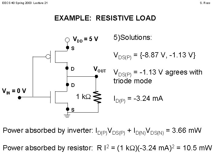
EECS 40 Spring 2003 Lecture 21 S. Ross EXAMPLE: RESISTIVE LOAD VDD = 5 V S VDS(P) = {-8. 87 V, -1. 13 V} VOUT D VIN = 0 V 5)Solutions: D 1 k. W VDS(P) = -1. 13 V agrees with triode mode ID(P) = -3. 24 m. A S Power absorbed by inverter: ID(P)VDS(P) + ID(N)VDS(N) = 3. 66 m. W Power absorbed by resistor: R I 2 = (1 k. W)(-3. 24 m. A)2 = 10. 5 m. W