A 3 D deep nwell CMOS MAPS for

- Slides: 1

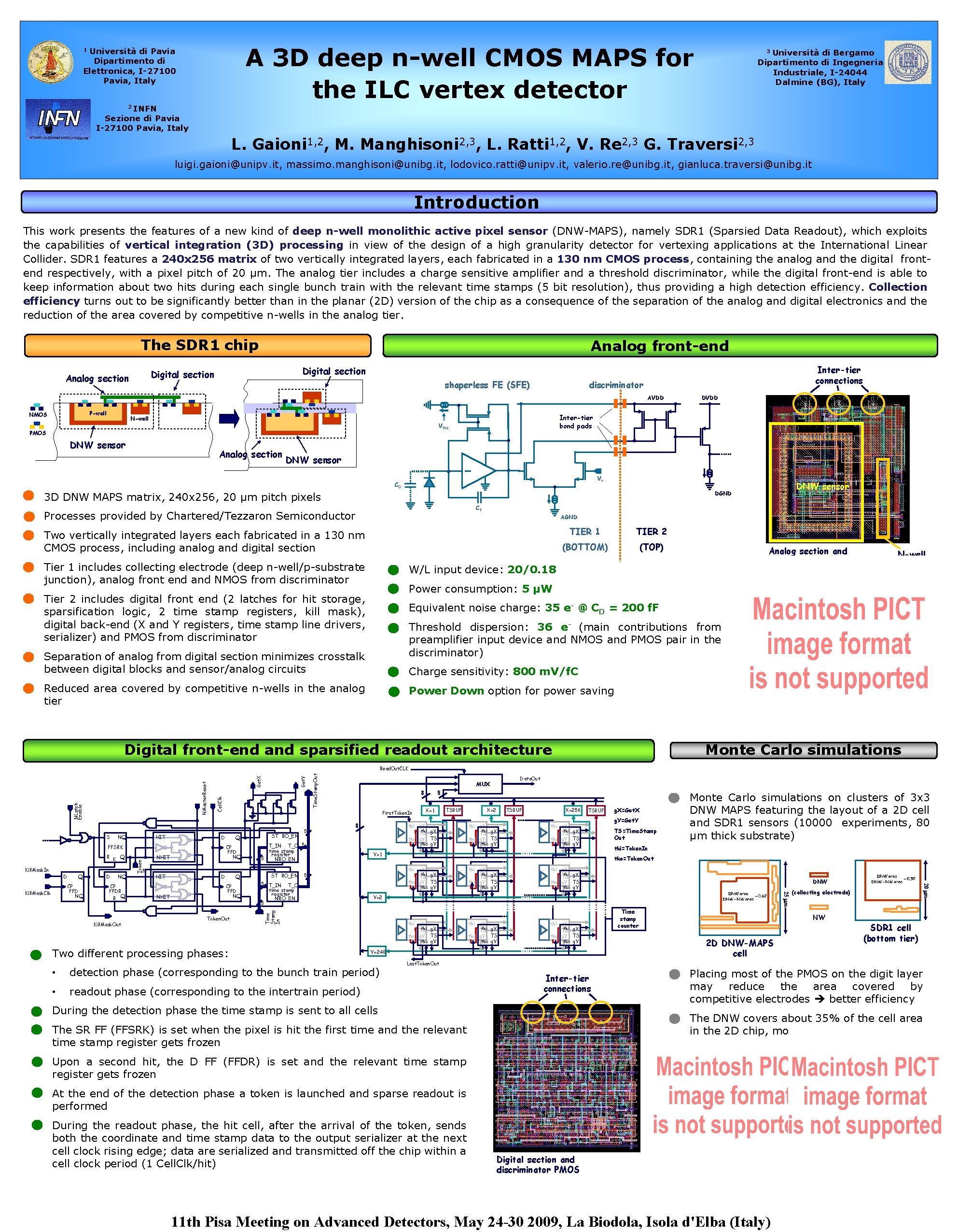
A 3 D deep n-well CMOS MAPS for the ILC vertex detector Università di Pavia Dipartimento di Elettronica, I-27100 Pavia, Italy 1 INFN Sezione di Pavia I-27100 Pavia, Italy Università di Bergamo Dipartimento di Ingegneria Industriale, I-24044 Dalmine (BG), Italy 3 2 L. Gaioni 1, 2, M. Manghisoni 2, 3, L. Ratti 1, 2, V. Re 2, 3 G. Traversi 2, 3 luigi. gaioni@unipv. it, massimo. manghisoni@unibg. it, lodovico. ratti@unipv. it, valerio. re@unibg. it, gianluca. traversi@unibg. it Introduction This work presents the features of a new kind of deep n-well monolithic active pixel sensor (DNW-MAPS), namely SDR 1 (Sparsied Data Readout), which exploits the capabilities of vertical integration (3 D) processing in view of the design of a high granularity detector for vertexing applications at the International Linear Collider. SDR 1 features a 240 x 256 matrix of two vertically integrated layers, each fabricated in a 130 nm CMOS process, containing the analog and the digital frontend respectively, with a pixel pitch of 20 μm. The analog tier includes a charge sensitive amplifier and a threshold discriminator, while the digital front-end is able to keep information about two hits during each single bunch train with the relevant time stamps (5 bit resolution), thus providing a high detection efficiency. Collection efficiency turns out to be significantly better than in the planar (2 D) version of the chip as a consequence of the separation of the analog and digital electronics and the reduction of the area covered by competitive n-wells in the analog tier. The SDR 1 chip Analog front-end Analog section Inter-tier connections Digital section shaperless FE (SFE) discriminator AVDD P-well NMOS N-well Inter-tier bond pads Vfbk PMOS DNW sensor Analog section DVDD DNW sensor Vt CD 3 D DNW MAPS matrix, 240 x 256, 20 μm pitch pixels • • Processes provided by Chartered/Tezzaron Semiconductor • Two vertically integrated layers each fabricated in a 130 nm CMOS process, including analog and digital section CF AGND Tier 1 includes collecting electrode (deep n-well/p-substrate junction), analog front end and NMOS from discriminator • Separation of analog from digital section minimizes crosstalk between digital blocks and sensor/analog circuits • Reduced area covered by competitive n-wells in the analog tier • TIER 1 TIER 2 (BOTTOM) (TOP) Analog section and discriminator NMOS W/L input device: 20/0. 18 • Tier 2 includes digital front end (2 latches for hit storage, sparsification logic, 2 time stamp registers, kill mask), digital back-end (X and Y registers, time stamp line drivers, serializer) and PMOS from discriminator • DNW sensor DGND N-well Preamplifier response to an 800 e- pulse • Power consumption: 5 μW • Equivalent noise charge: 35 e- @ CD = 200 f. F • Threshold dispersion: 36 e- (main contributions from preamplifier input device and NMOS and PMOS pair in the discriminator) • Charge sensitivity: 800 m. V/f. C • Power Down option for power saving Digital front-end and sparsified readout architecture Monte Carlo simulations NQ HIT R Kill. Mask. In D Q NQ CP FFDR Q R Kill. Mask. Out • NHIT Time. Stamp. Out Get. Y Get. X CP FFD NQ D Q CP FFD NQ Token. Out ST RO_EN 5 T_IN T_O 5 time stamp register 5 NRO_EN ST RO_EN Two different processing phases: TSBUF tki g. X TS tko g. Y X=256 TSBUF tki g. X TS tko g. Y Y=1 g. X=Get. X g. Y=Get. Y TS=Time. Stamp Out Monte Carlo simulations on clusters of 3 x 3 DNW MAPS featuring the layout of a 2 D cell and SDR 1 sensors (10000 experiments, 80 μm thick substrate) tki=Token. In tko=Token. Out tki g. X TS tko g. Y 5 5 T_IN T_O time stamp register NRO_EN 5 X=1 • tki g. X TS tko g. Y DNW Y=2 tki g. X TS tko g. Y tki g. X TS tko g. Y Time stamp counter Y=240 • detection phase (corresponding to the bunch train period) • readout phase (corresponding to the intertrain period) (collecting electrode) NW 2 D DNW-MAPS cell 20 mm Kill. Mask. Clk Q Q 8 5 25 mm CP FFD NQ D K Token In FFSRK 8 First. Token. In D Data. Out MUX Time Stamp In S Cell. Clk NLatch Enable NMaster. Reset Read. Out. CLK SDR 1 cell (bottom tier) Last. Token. Out • During the detection phase the time stamp is sent to all cells • The SR FF (FFSRK) is set when the pixel is hit the first time and the relevant time stamp register gets frozen • Upon a second hit, the D FF (FFDR) is set and the relevant time stamp register gets frozen • At the end of the detection phase a token is launched and sparse readout is performed • During the readout phase, the hit cell, after the arrival of the token, sends both the coordinate and time stamp data to the output serializer at the next cell clock rising edge; data are serialized and transmitted off the chip within a cell clock period (1 Cell. Clk/hit) Inter-tier connections • Placing most of the PMOS on the digit layer may reduce the area covered by competitive electrodes better efficiency • The DNW covers about 35% of the cell area in the 2 D chip, more than 50% in SDR 1 Digital section and discriminator PMOS 11 th Pisa Meeting on Advanced Detectors, May 24 -30 2009, La Biodola, Isola d'Elba (Italy)