A 12 GHz LowJitter LCVCO PLL in 130

- Slides: 1

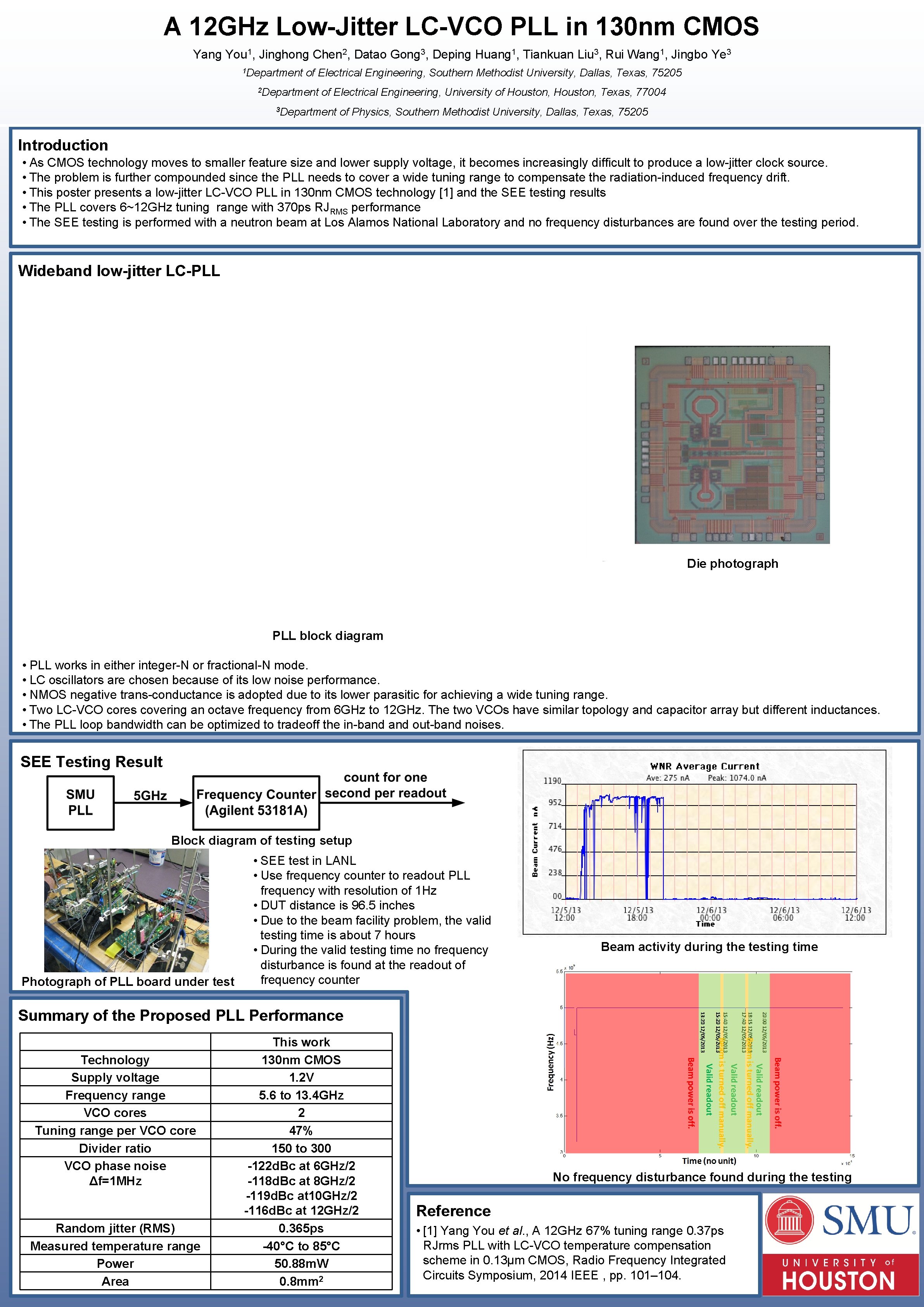
A 12 GHz Low-Jitter LC-VCO PLL in 130 nm CMOS Yang You 1, Jinghong Chen 2, Datao Gong 3, Deping Huang 1, Tiankuan Liu 3, Rui Wang 1, Jingbo Ye 3 1 Department of Electrical Engineering, Southern Methodist University, Dallas, Texas, 75205 2 Department of Electrical Engineering, University of Houston, Texas, 77004 3 Department of Physics, Southern Methodist University, Dallas, Texas, 75205 Introduction • As CMOS technology moves to smaller feature size and lower supply voltage, it becomes increasingly difficult to produce a low-jitter clock source. • The problem is further compounded since the PLL needs to cover a wide tuning range to compensate the radiation-induced frequency drift. • This poster presents a low-jitter LC-VCO PLL in 130 nm CMOS technology [1] and the SEE testing results • The PLL covers 6~12 GHz tuning range with 370 ps RJRMS performance • The SEE testing is performed with a neutron beam at Los Alamos National Laboratory and no frequency disturbances are found over the testing period. Wideband low-jitter LC-PLL Die photograph PLL block diagram • PLL works in either integer-N or fractional-N mode. • LC oscillators are chosen because of its low noise performance. • NMOS negative trans-conductance is adopted due to its lower parasitic for achieving a wide tuning range. • Two LC-VCO cores covering an octave frequency from 6 GHz to 12 GHz. The two VCOs have similar topology and capacitor array but different inductances. • The PLL loop bandwidth can be optimized to tradeoff the in-band out-band noises. SEE Testing Result Block diagram of testing setup Photograph of PLL board under test • SEE test in LANL • Use frequency counter to readout PLL frequency with resolution of 1 Hz • DUT distance is 96. 5 inches • Due to the beam facility problem, the valid testing time is about 7 hours • During the valid testing time no frequency disturbance is found at the readout of frequency counter Beam activity during the testing time Summary of the Proposed PLL Performance Technology Supply voltage Frequency range VCO cores Tuning range per VCO core Divider ratio VCO phase noise Δf=1 MHz Random jitter (RMS) Measured temperature range Power Area This work 130 nm CMOS 1. 2 V 5. 6 to 13. 4 GHz 2 47% 150 to 300 -122 d. Bc at 6 GHz/2 -118 d. Bc at 8 GHz/2 -119 d. Bc at 10 GHz/2 -116 d. Bc at 12 GHz/2 0. 365 ps -40°C to 85°C 50. 88 m. W 0. 8 mm 2 No frequency disturbance found during the testing Reference • [1] Yang You et al. , A 12 GHz 67% tuning range 0. 37 ps RJrms PLL with LC-VCO temperature compensation scheme in 0. 13μm CMOS, Radio Frequency Integrated Circuits Symposium, 2014 IEEE , pp. 101– 104.