Zynq Architecture 7 Series FPGA Architecture Cristian Sisterna




- Slides: 67

Zynq Architecture 7 -Series FPGA Architecture Cristian Sisterna Universidad Nacional de San Juan Argentina

7 -Series FPGA Architecture 7 -Series Xilinx FPGAs ICTP 2

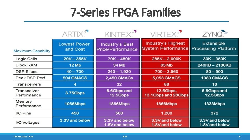
7 -Series FPGA Families 7 -Series Xilinx FPGAs ICTP 3

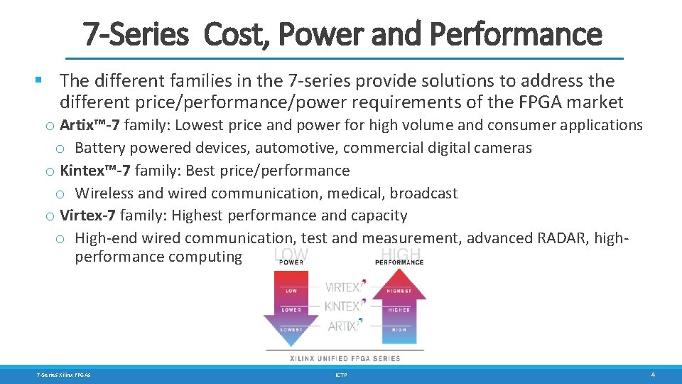
7 -Series Cost, Power and Performance § The different families in the 7 -series provide solutions to address the different price/performance/power requirements of the FPGA market o Artix™-7 family: Lowest price and power for high volume and consumer applications o Battery powered devices, automotive, commercial digital cameras o Kintex™-7 family: Best price/performance o Wireless and wired communication, medical, broadcast o Virtex-7 family: Highest performance and capacity o High-end wired communication, test and measurement, advanced RADAR, highperformance computing 7 -Series Xilinx FPGAs ICTP 4

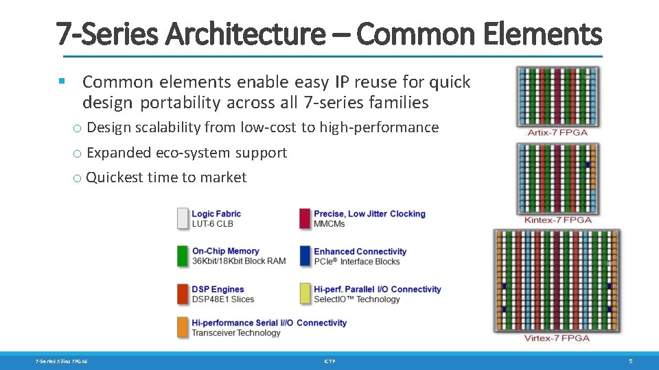
7 -Series Architecture – Common Elements § Common elements enable easy IP reuse for quick design portability across all 7 -series families o Design scalability from low-cost to high-performance o Expanded eco-system support o Quickest time to market 7 -Series Xilinx FPGAs ICTP 5

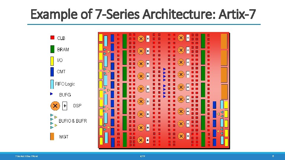
Example of 7 -Series Architecture: Artix-7 7 -Series Xilinx FPGAs ICTP 6

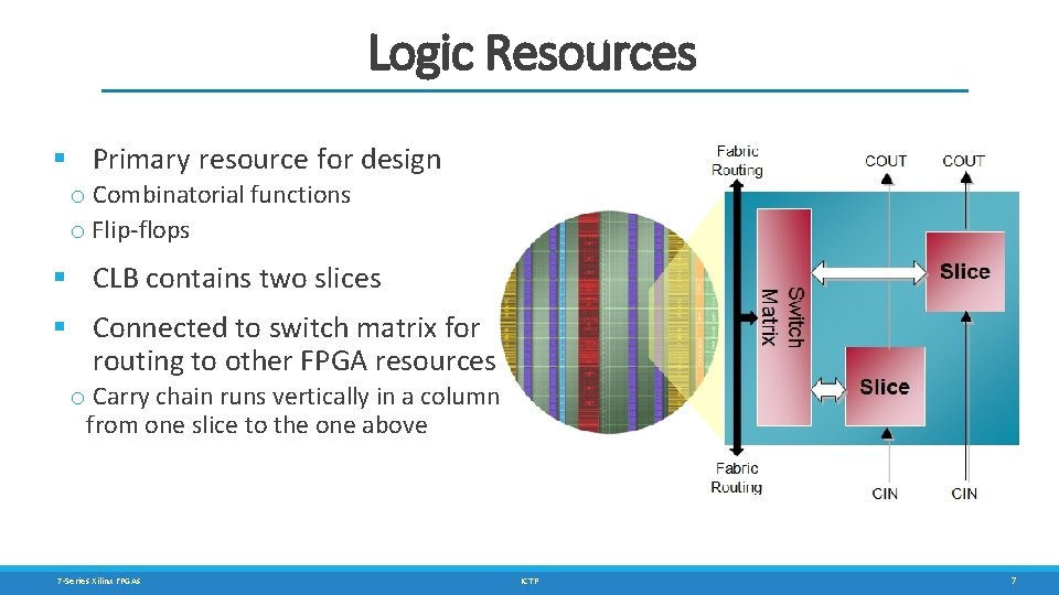
Logic Resources § Primary resource for design o Combinatorial functions o Flip-flops § CLB contains two slices § Connected to switch matrix for routing to other FPGA resources o Carry chain runs vertically in a column from one slice to the one above 7 -Series Xilinx FPGAs ICTP 7

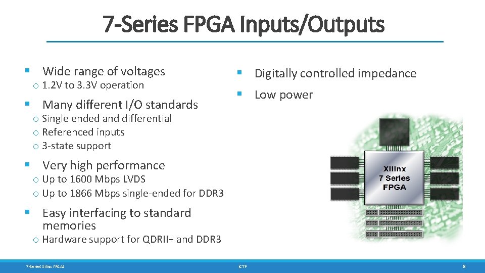
7 -Series FPGA Inputs/Outputs § Wide range of voltages o 1. 2 V to 3. 3 V operation § Many different I/O standards § Digitally controlled impedance § Low power o Single ended and differential o Referenced inputs o 3 -state support § Very high performance o Up to 1600 Mbps LVDS o Up to 1866 Mbps single-ended for DDR 3 § Easy interfacing to standard memories o Hardware support for QDRII+ and DDR 3 7 -Series Xilinx FPGAs ICTP 8

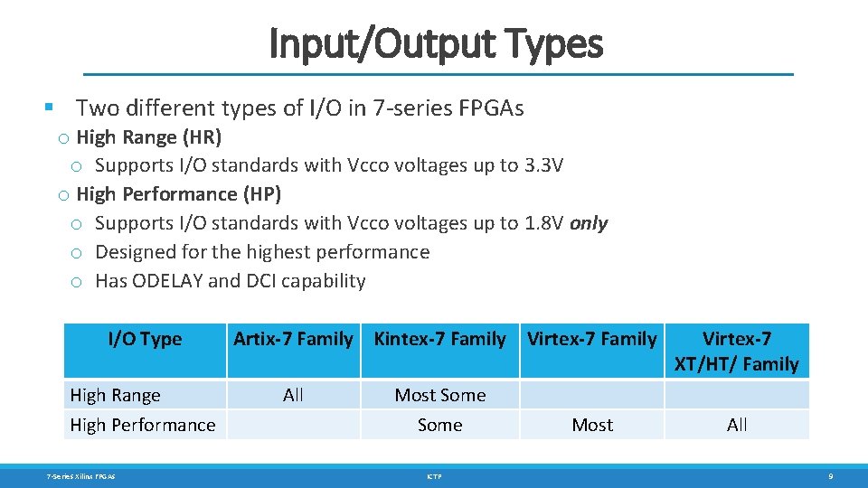
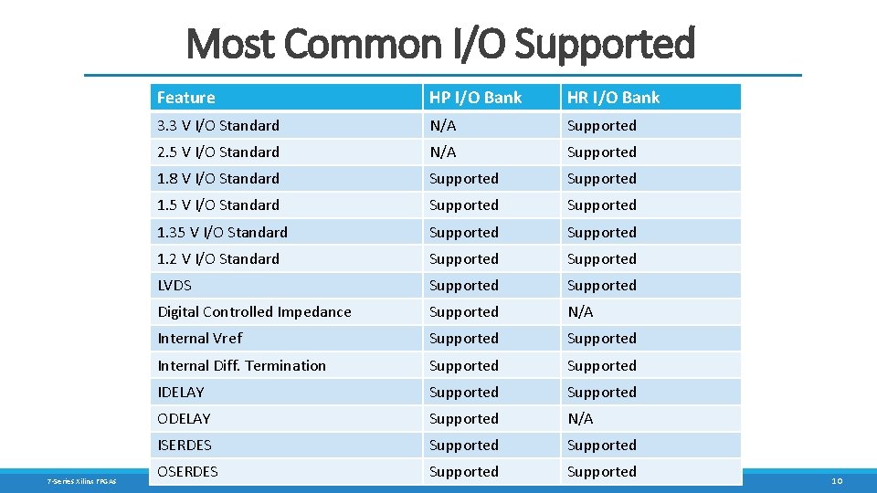
Input/Output Types § Two different types of I/O in 7 -series FPGAs o High Range (HR) o Supports I/O standards with Vcco voltages up to 3. 3 V o High Performance (HP) o Supports I/O standards with Vcco voltages up to 1. 8 V only o Designed for the highest performance o Has ODELAY and DCI capability I/O Type High Range High Performance 7 -Series Xilinx FPGAs Artix-7 Family Kintex-7 Family Virtex-7 Family All Virtex-7 XT/HT/ Family Most Some ICTP Most All 9

Most Common I/O Supported 7 -Series Xilinx FPGAs Feature HP I/O Bank HR I/O Bank 3. 3 V I/O Standard N/A Supported 2. 5 V I/O Standard N/A Supported 1. 8 V I/O Standard Supported 1. 5 V I/O Standard Supported 1. 35 V I/O Standard Supported 1. 2 V I/O Standard Supported LVDS Supported Digital Controlled Impedance Supported N/A Internal Vref Supported Internal Diff. Termination Supported IDELAY Supported ODELAY Supported N/A ISERDES Supported OSERDES Supported ICTP Supported 10

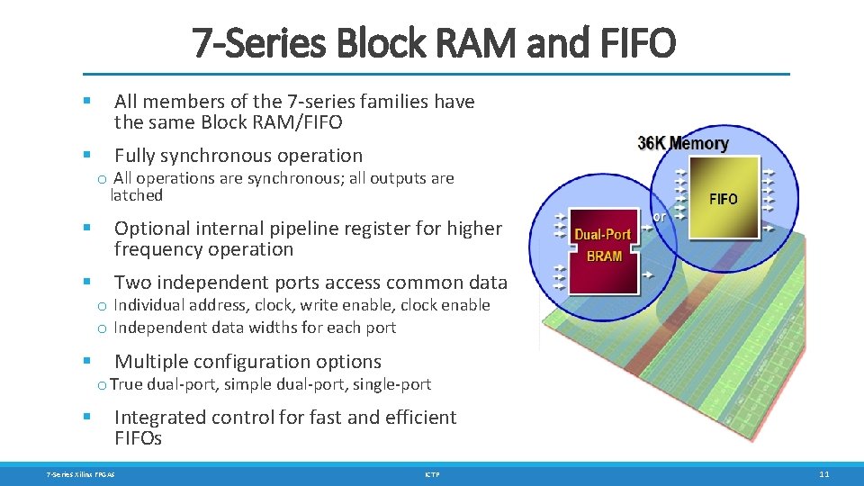
7 -Series Block RAM and FIFO § All members of the 7 -series families have the same Block RAM/FIFO § Fully synchronous operation o All operations are synchronous; all outputs are latched § Optional internal pipeline register for higher frequency operation § Two independent ports access common data § § o Individual address, clock, write enable, clock enable o Independent data widths for each port Multiple configuration options o True dual-port, simple dual-port, single-port Integrated control for fast and efficient FIFOs 7 -Series Xilinx FPGAs ICTP 11

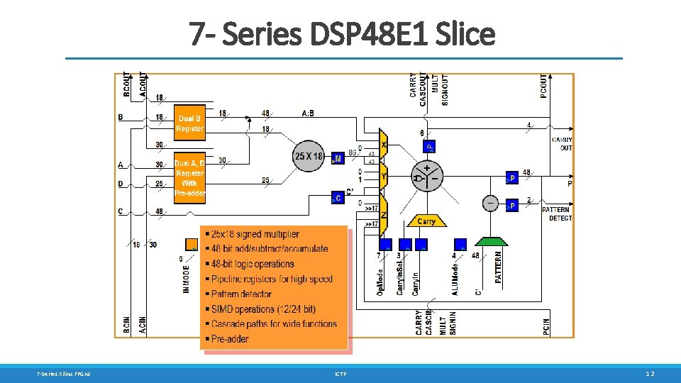
7 - Series DSP 48 E 1 Slice 7 -Series Xilinx FPGAs ICTP 12

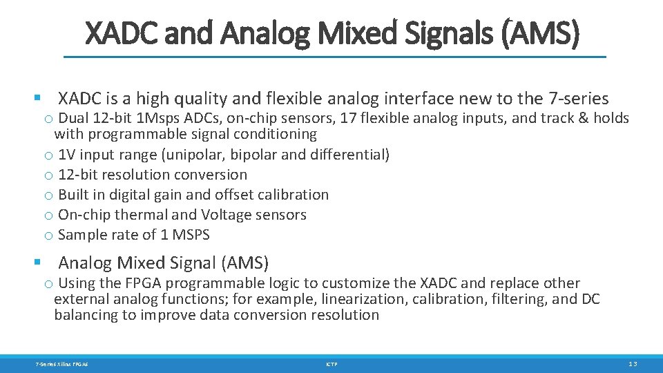
XADC and Analog Mixed Signals (AMS) § XADC is a high quality and flexible analog interface new to the 7 -series o Dual 12 -bit 1 Msps ADCs, on-chip sensors, 17 flexible analog inputs, and track & holds with programmable signal conditioning o 1 V input range (unipolar, bipolar and differential) o 12 -bit resolution conversion o Built in digital gain and offset calibration o On-chip thermal and Voltage sensors o Sample rate of 1 MSPS § Analog Mixed Signal (AMS) o Using the FPGA programmable logic to customize the XADC and replace other external analog functions; for example, linearization, calibration, filtering, and DC balancing to improve data conversion resolution 7 -Series Xilinx FPGAs ICTP 13

Zynq Architecture 7 -Series Xilinx FPGAs ICTP 14

Zynq-7000 Main Features § Complete ARM®-based processing system o Application Processor Unit (APU) o Dual ARM Cortex™-A 9 processors o Caches and support blocks o Fully integrated memory controllers o I/O peripherals § Tightly integrated programmable logic o Used to extend the processing system o Scalable density and performance § Flexible array of I/O o Wide range of external multi-standard I/O o High-performance integrated serial transceivers o Analog-to-digital converter inputs 7 -Series Xilinx FPGAs ICTP 15

ARM Processor Architecture § ARM Cortex-A 9 processor implements the ARMv 7 -A architecture o ARMv 7 is the ARM Instruction Set Architecture (ISA) o Thumb instructions: 16 bits; Thumb-2 instructions: 32 bits o NEON: ARM’s Single Instruction Multiple Data (SIMD) instructions o ARMv 7 -A: Application set that includes support for a Memory Management Unit (MMU) o ARMv 7 -R: Real-time set that includes support for a Memory Protection Unit (MPU) o ARMv 7 -M: Microcontroller set that is the smallest set § ARM Advanced Microcontroller Bus Architecture (AMBA®) protocol o AXI 3: Third-generation ARM interface o AXI 4: Adding to the existing AXI definition (extended bursts, subsets) § Cortex is the new family of processors o ARM family is older generation; Cortex is current; MMUs in Cortex processors and MPUs in ARM 7 -Series Xilinx FPGAs ICTP 16

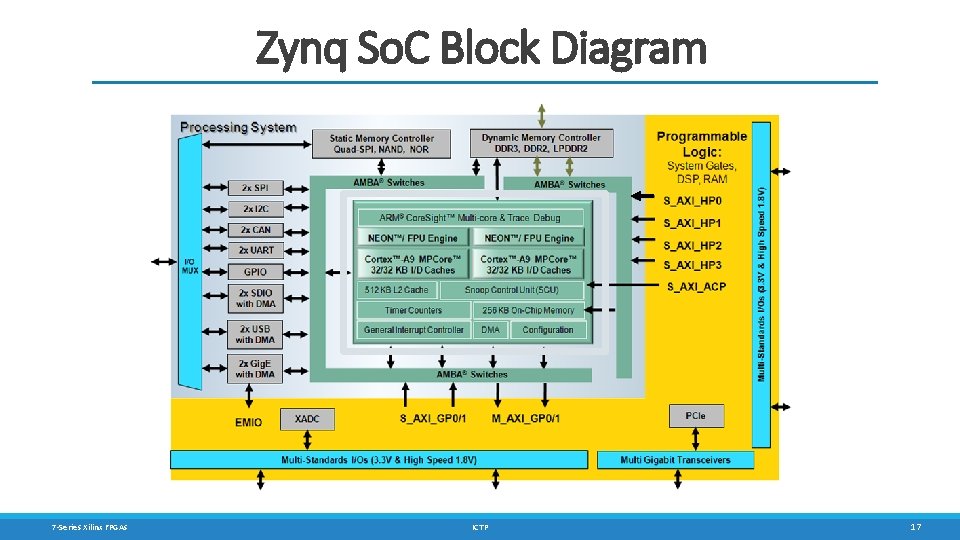
Zynq So. C Block Diagram 7 -Series Xilinx FPGAs ICTP 17

PS Main Components § Application processing unit (APU) § I/O peripherals (IOP) o Multiplexed I/O (MIO), extended multiplexed I/O (EMIO) § § Memory interfaces PS interconnect DMA Timers o Public and private § General interrupt controller (GIC) § On-chip memory (OCM): RAM § Debug controller: Core. Sight 7 -Series Xilinx FPGAs ICTP 18

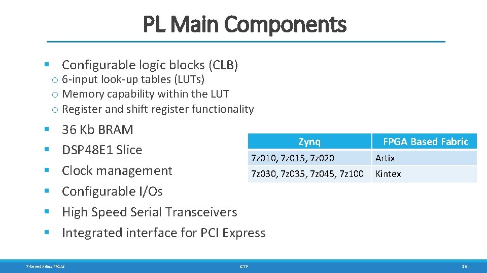
PL Main Components § Configurable logic blocks (CLB) o 6 -input look-up tables (LUTs) o Memory capability within the LUT o Register and shift register functionality § § § 36 Kb BRAM Zynq DSP 48 E 1 Slice 7 z 010, 7 z 015, 7 z 020 Clock management 7 z 030, 7 z 035, 7 z 045, 7 z 100 Configurable I/Os High Speed Serial Transceivers Integrated interface for PCI Express 7 -Series Xilinx FPGAs ICTP FPGA Based Fabric Artix Kintex 19

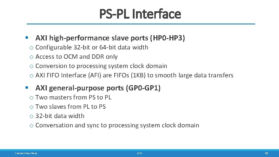
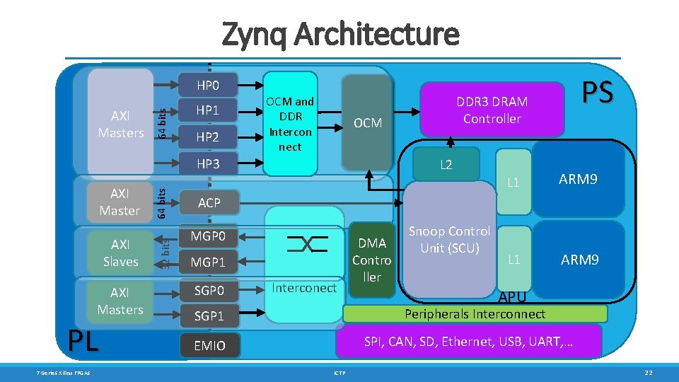
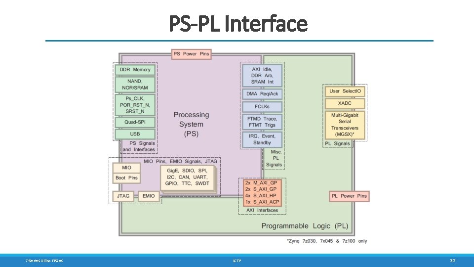
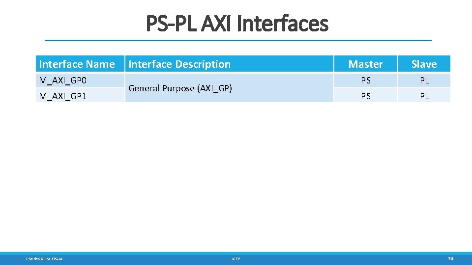
PS-PL Interface § AXI high-performance slave ports (HP 0 -HP 3) o Configurable 32 -bit or 64 -bit data width o Access to OCM and DDR only o Conversion to processing system clock domain o AXI FIFO Interface (AFI) are FIFOs (1 KB) to smooth large data transfers § AXI general-purpose ports (GP 0 -GP 1) o Two masters from PS to PL o Two slaves from PL to PS o 32 -bit data width o Conversation and sync to processing system clock domain 7 -Series Xilinx FPGAs ICTP 20

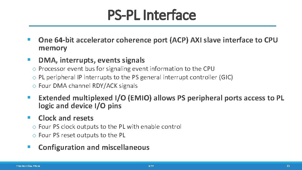
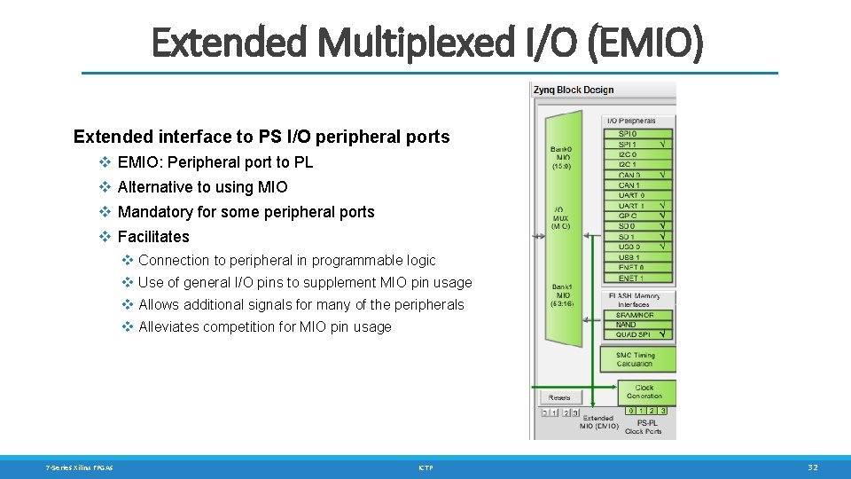
PS-PL Interface § One 64 -bit accelerator coherence port (ACP) AXI slave interface to CPU memory § DMA, interrupts, events signals o Processor event bus for signaling event information to the CPU o PL peripheral IP interrupts to the PS general interrupt controller (GIC) o Four DMA channel RDY/ACK signals § Extended multiplexed I/O (EMIO) allows PS peripheral ports access to PL logic and device I/O pins § Clock and resets o Four PS clock outputs to the PL with enable control o Four PS reset outputs to the PL § Configuration and miscellaneous 7 -Series Xilinx FPGAs ICTP 21

Zynq Architecture AXI Masters 64 bits HP 0 HP 1 HP 2 OCM and DDR Intercon nect OCM AXI Slaves AXI Masters PL 7 -Series Xilinx FPGAs 32 bits AXI Master 64 bits HP 3 PS DDR 3 DRAM Controller L 2 L 1 ARM 9 ACP MGP 0 MGP 1 SGP 0 Interconect DMA Contro ller Snoop Control Unit (SCU) APU Peripherals Interconnect SGP 1 SPI, CAN, SD, Ethernet, USB, UART, … EMIO ICTP 22

PS-PL Interface 7 -Series Xilinx FPGAs ICTP 23

PS-PL AXI Interfaces Interface Name M_AXI_GP 0 M_AXI_GP 1 S_AXI_GPO S_AXI_GP 1 S_AXI_ACP S_AXI_HP 0 S_AXI_HP 1 S_AXI_HP 2 S_AXI_HP 3 7 -Series Xilinx FPGAs Interface Description General Purpose (AXI_GP) Accelerator Coherence Port High Performance Ports (AXI_HP)with read/write FIFOs and two dedicated memory ports on DDR controller and a path to the OCM ICTP Master Slave PS PL PL PS PL PS 24

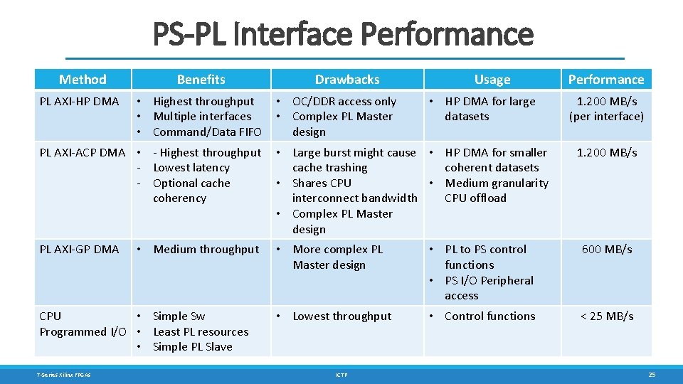
PS-PL Interface Performance Method Benefits PL AXI-HP DMA • Highest throughput • Multiple interfaces • Command/Data FIFO Drawbacks • OC/DDR access only • Complex PL Master design Usage • HP DMA for large datasets Performance 1. 200 MB/s (per interface) PL AXI-ACP DMA • - Highest throughput - Lowest latency - Optional cache coherency • Large burst might cause • HP DMA for smaller cache trashing coherent datasets • Shares CPU • Medium granularity interconnect bandwidth CPU offload • Complex PL Master design PL AXI-GP DMA • More complex PL Master design • PL to PS control functions • PS I/O Peripheral access 600 MB/s • Lowest throughput • Control functions < 25 MB/s • Medium throughput CPU • Simple Sw Programmed I/O • Least PL resources • Simple PL Slave 7 -Series Xilinx FPGAs ICTP 1. 200 MB/s 25

PS-PL Miscellaneous Signals § PL Clocks and Resets § PL Interrupts to PS § IOP Interrupts to PL § Events § Idle AXI, DDR, ARB, SRAM Interrupt § DMA Controller § EMIO Signals 7 -Series Xilinx FPGAs ICTP 26

PS Peripherals and Connections 7 -Series Xilinx FPGAs ICTP 27

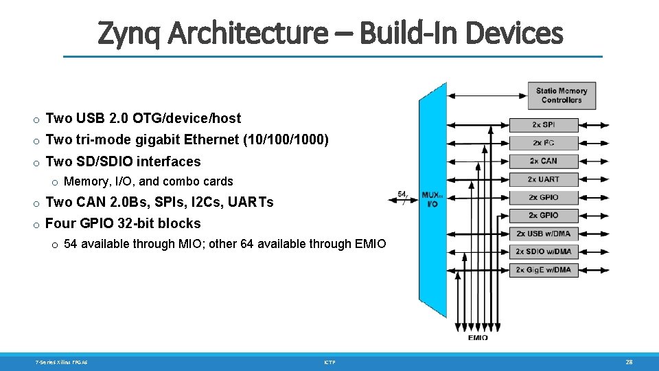
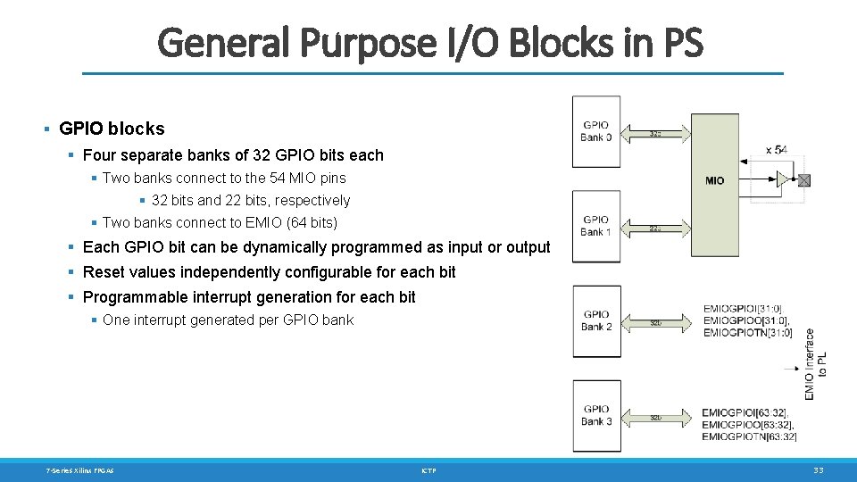
Zynq Architecture – Build-In Devices o Two USB 2. 0 OTG/device/host o Two tri-mode gigabit Ethernet (10/1000) o Two SD/SDIO interfaces o Memory, I/O, and combo cards o Two CAN 2. 0 Bs, SPIs, I 2 Cs, UARTs o Four GPIO 32 -bit blocks o 54 available through MIO; other 64 available through EMIO 7 -Series Xilinx FPGAs ICTP 28

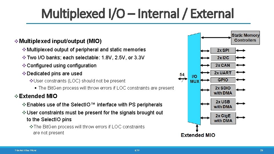
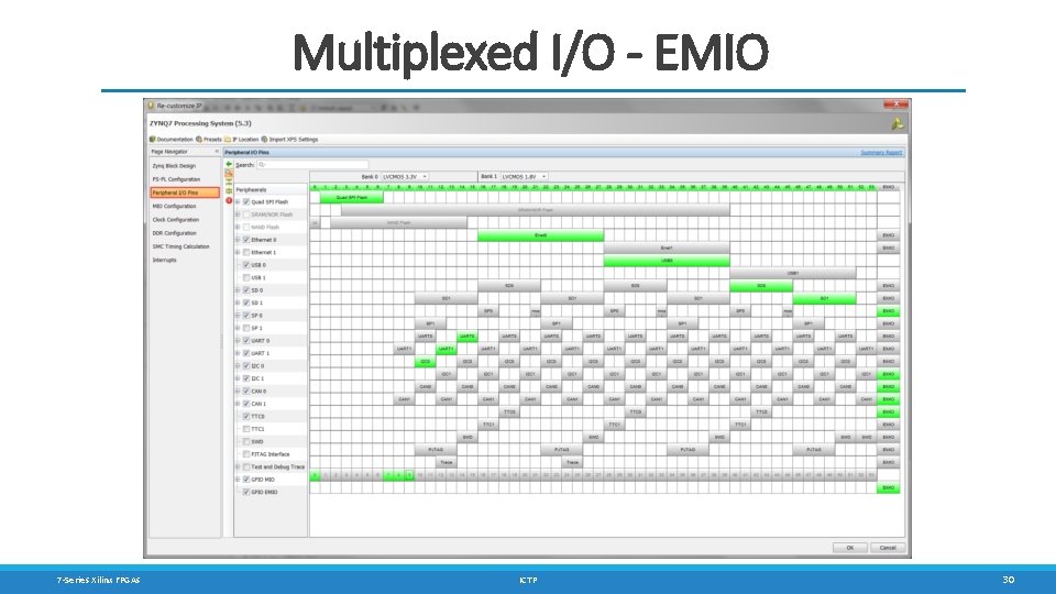
Multiplexed I/O – Internal / External v Multiplexed input/output (MIO) v Multiplexed output of peripheral and static memories v Two I/O banks; each selectable: 1. 8 V, 2. 5 V, or 3. 3 V v Configured using configuration v Dedicated pins are used v. User constraints (LOC) should not be present § The Bit. Gen process will throw errors if LOC constraints are present v Extended MIO v Enables use of the Select. IO™ interface with PS peripherals v User constraints must be present for the signals brought out to the Select. IO pins v. The Bit. Gen process will throw errors if LOC constraints are not present 7 -Series Xilinx FPGAs ICTP 29

Multiplexed I/O - EMIO 7 -Series Xilinx FPGAs ICTP 30

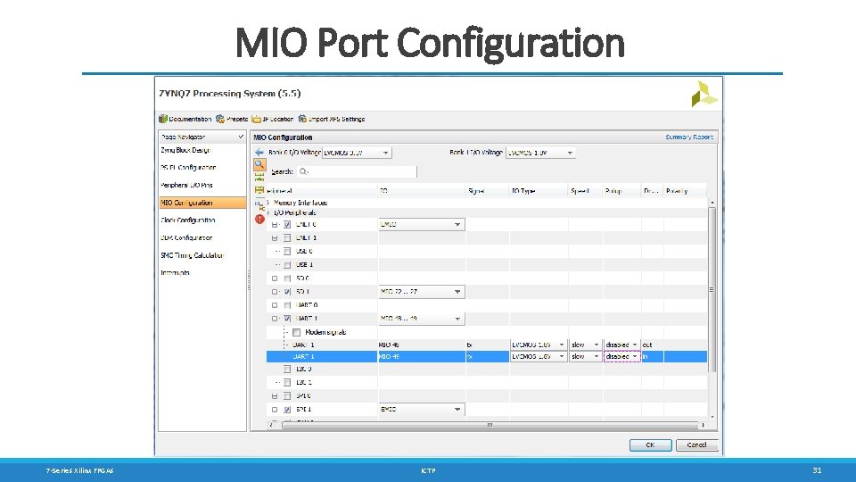
MIO Port Configuration 7 -Series Xilinx FPGAs ICTP 31

Extended Multiplexed I/O (EMIO) Extended interface to PS I/O peripheral ports v EMIO: Peripheral port to PL v Alternative to using MIO v Mandatory for some peripheral ports v Facilitates v Connection to peripheral in programmable logic v Use of general I/O pins to supplement MIO pin usage v Allows additional signals for many of the peripherals v Alleviates competition for MIO pin usage 7 -Series Xilinx FPGAs ICTP 32

General Purpose I/O Blocks in PS § GPIO blocks § Four separate banks of 32 GPIO bits each § Two banks connect to the 54 MIO pins § 32 bits and 22 bits, respectively § Two banks connect to EMIO (64 bits) § Each GPIO bit can be dynamically programmed as input or output § Reset values independently configurable for each bit § Programmable interrupt generation for each bit § One interrupt generated per GPIO bank 7 -Series Xilinx FPGAs ICTP 33

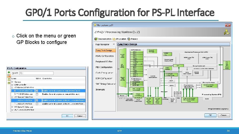
GP 0/1 Ports Configuration for PS-PL Interface o Click on the menu or green GP Blocks to configure 7 -Series Xilinx FPGAs ICTP 34

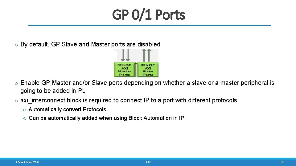
GP 0/1 Ports o By default, GP Slave and Master ports are disabled o Enable GP Master and/or Slave ports depending on whether a slave or a master peripheral is going to be added in PL o axi_interconnect block is required to connect IP to a port with different protocols o Automatically convert Protocols o Can be automatically added when using Block Automation in IPI 7 -Series Xilinx FPGAs ICTP 35

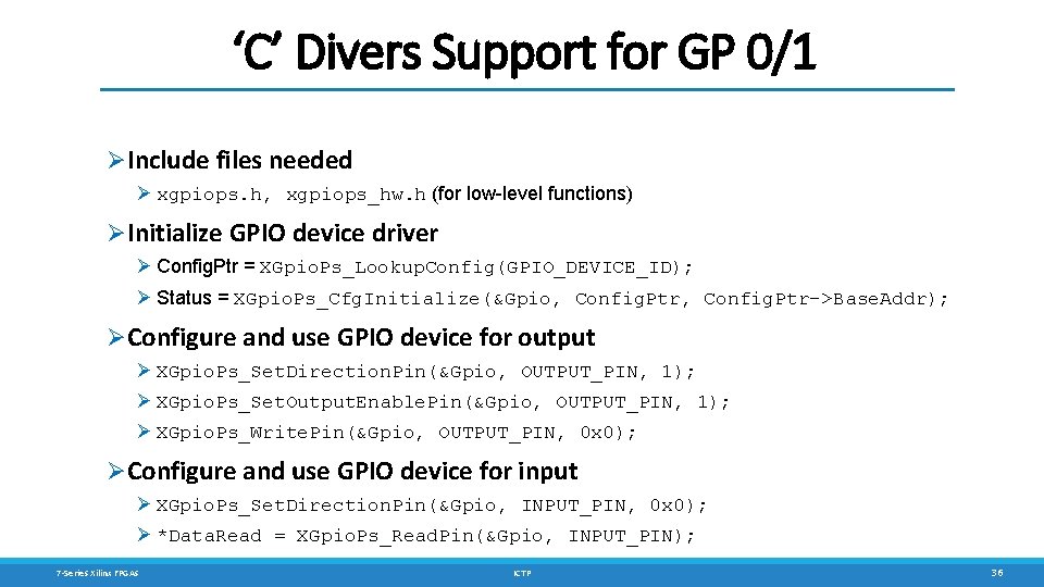
‘C’ Divers Support for GP 0/1 ØInclude files needed Ø xgpiops. h, xgpiops_hw. h (for low-level functions) ØInitialize GPIO device driver Ø Config. Ptr = XGpio. Ps_Lookup. Config(GPIO_DEVICE_ID); Ø Status = XGpio. Ps_Cfg. Initialize(&Gpio, Config. Ptr->Base. Addr); ØConfigure and use GPIO device for output Ø XGpio. Ps_Set. Direction. Pin(&Gpio, OUTPUT_PIN, 1); Ø XGpio. Ps_Set. Output. Enable. Pin(&Gpio, OUTPUT_PIN, 1); Ø XGpio. Ps_Write. Pin(&Gpio, OUTPUT_PIN, 0 x 0); ØConfigure and use GPIO device for input Ø XGpio. Ps_Set. Direction. Pin(&Gpio, INPUT_PIN, 0 x 0); Ø *Data. Read = XGpio. Ps_Read. Pin(&Gpio, INPUT_PIN); 7 -Series Xilinx FPGAs ICTP 36

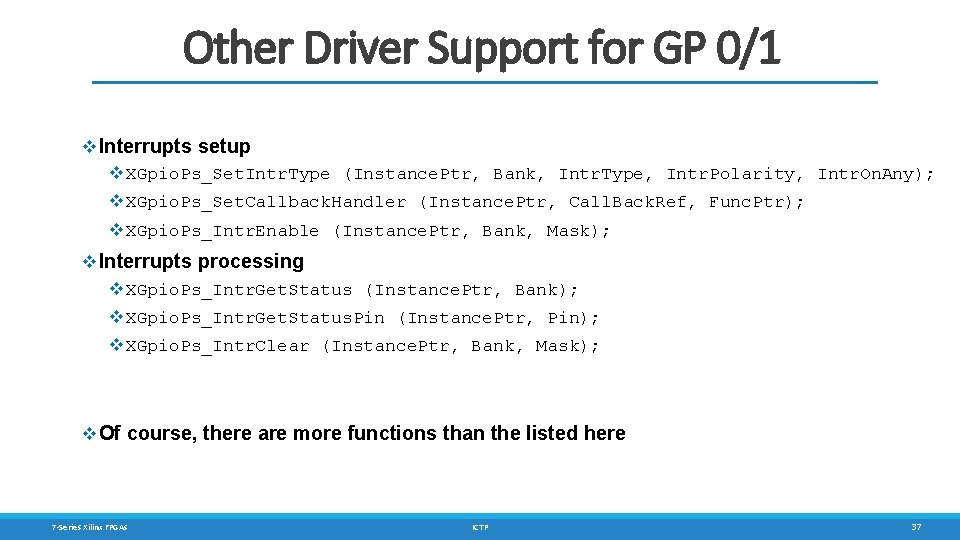
Other Driver Support for GP 0/1 v Interrupts setup v XGpio. Ps_Set. Intr. Type (Instance. Ptr, Bank, Intr. Type, Intr. Polarity, Intr. On. Any); v XGpio. Ps_Set. Callback. Handler (Instance. Ptr, Call. Back. Ref, Func. Ptr); v XGpio. Ps_Intr. Enable (Instance. Ptr, Bank, Mask); v Interrupts processing v XGpio. Ps_Intr. Get. Status (Instance. Ptr, Bank); v XGpio. Ps_Intr. Get. Status. Pin (Instance. Ptr, Pin); v XGpio. Ps_Intr. Clear (Instance. Ptr, Bank, Mask); v Of course, there are more functions than the listed here 7 -Series Xilinx FPGAs ICTP 37

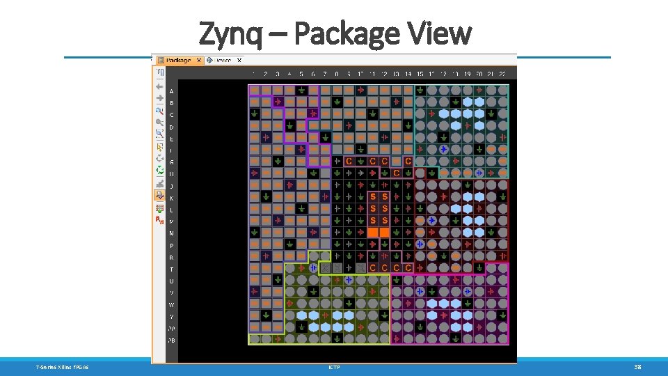
Zynq – Package View 7 -Series Xilinx FPGAs ICTP 38

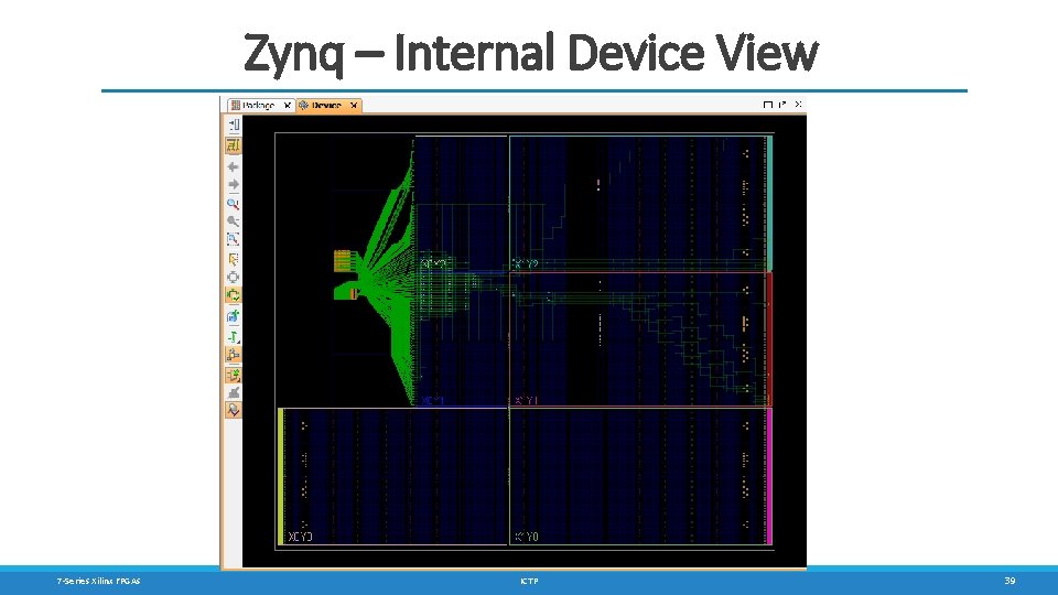
Zynq – Internal Device View 7 -Series Xilinx FPGAs ICTP 39

Apendix

IO Peripherals 7 -Series Xilinx FPGAs ICTP 41

I 2 C § I²C bus specification version 2 § Programmable to use normal (7 -bit) or extended (10 -bit) addressing § Programmable rates: fast mode (400 kbit/s) , standard (10 0 kbits/s), and low (10 kbits/s) o Rates higher than 400 kbits/sec are not supported § Programmable as either a master or slave interface § Capable of clock synchronization and bus arbitration § Fully programmable slave response address § Reversible FIFO operation supported § 16 -byte buffer size § Slave monitor mode when set up as master § I²C bus hold for slow host service § Slave timeout detection with programmable period § Transfer status interrupts and flags 7 -Series Xilinx FPGAs ICTP 42

CAN § § § Up to 24 -MHz CAN_REF clock as system clock 64 message-deep receiver and transmitter buffer Full CAN 2. 0 B compliant; conforms to ISO 11898 -1 Maximum baud rate of 1 Mb/s Four message filters required for buffer mode Listen-only mode for test and debug External PHY I/O “Wake-on-message” Time-stamping for receive messages TX and RX FIFO watermarking Exception: no power-down mode 7 -Series Xilinx FPGAs ICTP 43

SD-SDIO § Support for version 2. 0 of SD Specification § Full-speed (4 MB/s) and low-speed (2 MB/s) support o Low-speed clock (400 KHz) used until bandwidth negotiated § § § § 1 -bit and 4 -bit data interface support Host mode support only Built-in DMA controller Full-speed clock (0 -50 MHz) with maximum throughput at 25 MB/s 1 KB data FIFO interface Support for MMC 3. 31 card at 52 MHz Support for memory, I/O, and combo cards Support for power control modes and interrupts 7 -Series Xilinx FPGAs ICTP 44

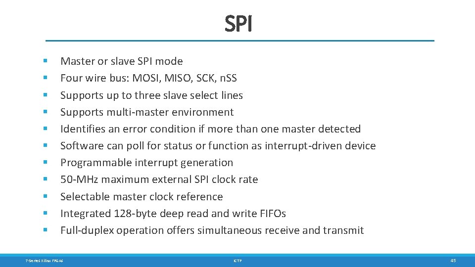
SPI § § § Master or slave SPI mode Four wire bus: MOSI, MISO, SCK, n. SS Supports up to three slave select lines Supports multi-master environment Identifies an error condition if more than one master detected Software can poll for status or function as interrupt-driven device Programmable interrupt generation 50 -MHz maximum external SPI clock rate Selectable master clock reference Integrated 128 -byte deep read and write FIFOs Full-duplex operation offers simultaneous receive and transmit 7 -Series Xilinx FPGAs ICTP 45

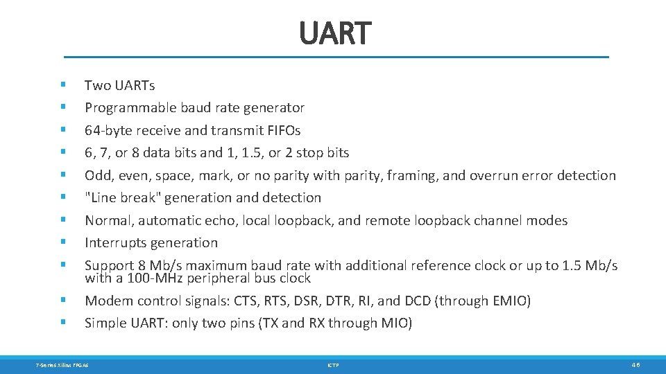
UART § § § Two UARTs Programmable baud rate generator 64 -byte receive and transmit FIFOs 6, 7, or 8 data bits and 1, 1. 5, or 2 stop bits Odd, even, space, mark, or no parity with parity, framing, and overrun error detection "Line break" generation and detection Normal, automatic echo, local loopback, and remote loopback channel modes Interrupts generation Support 8 Mb/s maximum baud rate with additional reference clock or up to 1. 5 Mb/s with a 100 -MHz peripheral bus clock Modem control signals: CTS, RTS, DSR, DTR, RI, and DCD (through EMIO) Simple UART: only two pins (TX and RX through MIO) 7 -Series Xilinx FPGAs ICTP 46

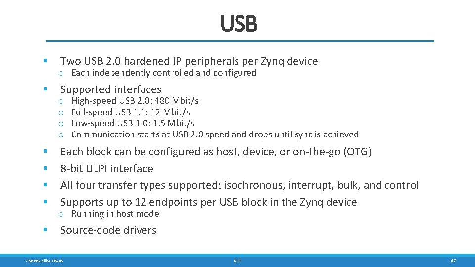
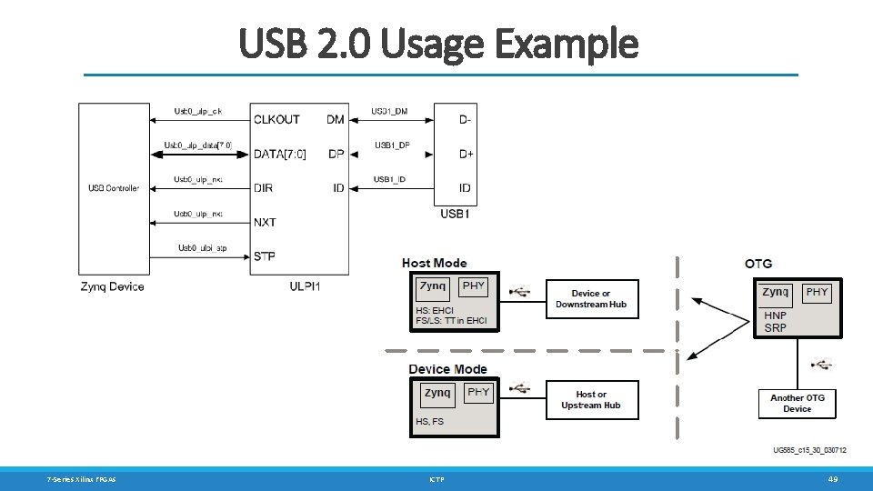
USB § § § § Two USB 2. 0 hardened IP peripherals per Zynq device o Each independently controlled and configured Supported interfaces o o High-speed USB 2. 0: 480 Mbit/s Full-speed USB 1. 1: 12 Mbit/s Low-speed USB 1. 0: 1. 5 Mbit/s Communication starts at USB 2. 0 speed and drops until sync is achieved Each block can be configured as host, device, or on-the-go (OTG) 8 -bit ULPI interface All four transfer types supported: isochronous, interrupt, bulk, and control Supports up to 12 endpoints per USB block in the Zynq device o Running in host mode Source-code drivers 7 -Series Xilinx FPGAs ICTP 47

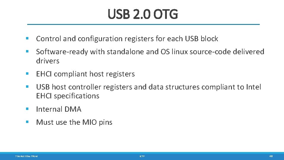
USB 2. 0 OTG § Control and configuration registers for each USB block § Software-ready with standalone and OS linux source-code delivered drivers § EHCI compliant host registers § USB host controller registers and data structures compliant to Intel EHCI specifications § Internal DMA § Must use the MIO pins 7 -Series Xilinx FPGAs ICTP 48

USB 2. 0 Usage Example 7 -Series Xilinx FPGAs ICTP 49

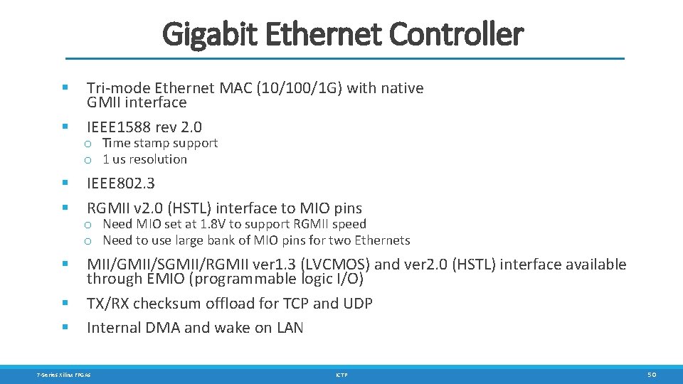
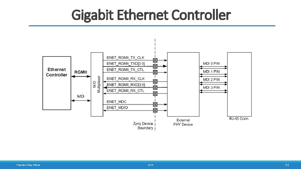
Gigabit Ethernet Controller § § § § Tri-mode Ethernet MAC (10/100/1 G) with native GMII interface IEEE 1588 rev 2. 0 o Time stamp support o 1 us resolution IEEE 802. 3 RGMII v 2. 0 (HSTL) interface to MIO pins o Need MIO set at 1. 8 V to support RGMII speed o Need to use large bank of MIO pins for two Ethernets MII/GMII/SGMII/RGMII ver 1. 3 (LVCMOS) and ver 2. 0 (HSTL) interface available through EMIO (programmable logic I/O) TX/RX checksum offload for TCP and UDP Internal DMA and wake on LAN 7 -Series Xilinx FPGAs ICTP 50

Gigabit Ethernet Controller 7 -Series Xilinx FPGAs ICTP 51

Application Processor Unit (APU) 7 -Series Xilinx FPGAs ICTP 52

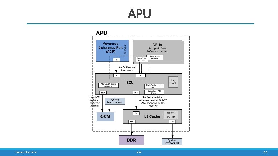
APU 7 -Series Xilinx FPGAs ICTP 53

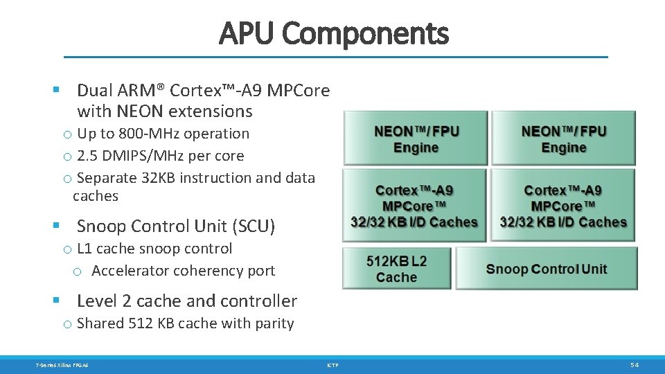
APU Components § Dual ARM® Cortex™-A 9 MPCore with NEON extensions o Up to 800 -MHz operation o 2. 5 DMIPS/MHz per core o Separate 32 KB instruction and data caches § Snoop Control Unit (SCU) o L 1 cache snoop control o Accelerator coherency port § Level 2 cache and controller o Shared 512 KB cache with parity 7 -Series Xilinx FPGAs ICTP 54

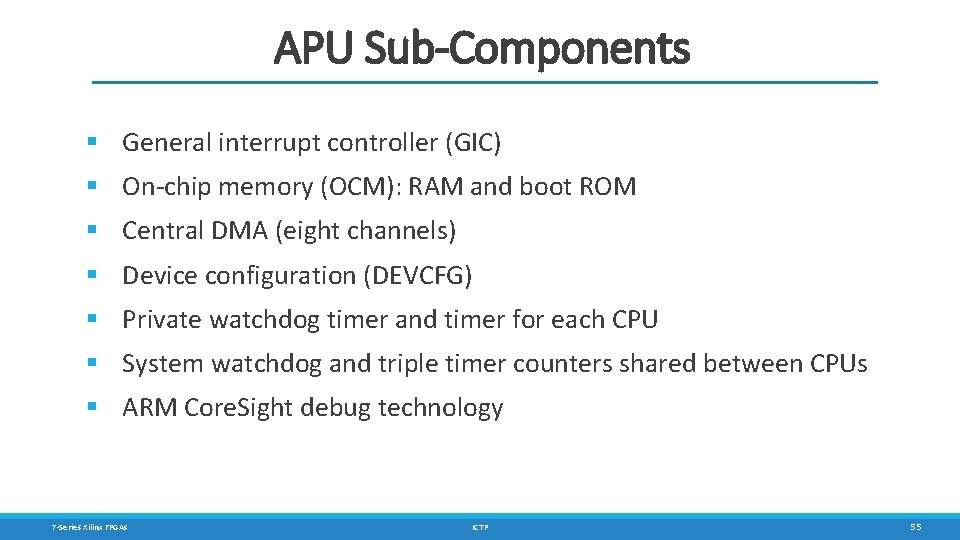
APU Sub-Components § General interrupt controller (GIC) § On-chip memory (OCM): RAM and boot ROM § Central DMA (eight channels) § Device configuration (DEVCFG) § Private watchdog timer and timer for each CPU § System watchdog and triple timer counters shared between CPUs § ARM Core. Sight debug technology 7 -Series Xilinx FPGAs ICTP 55

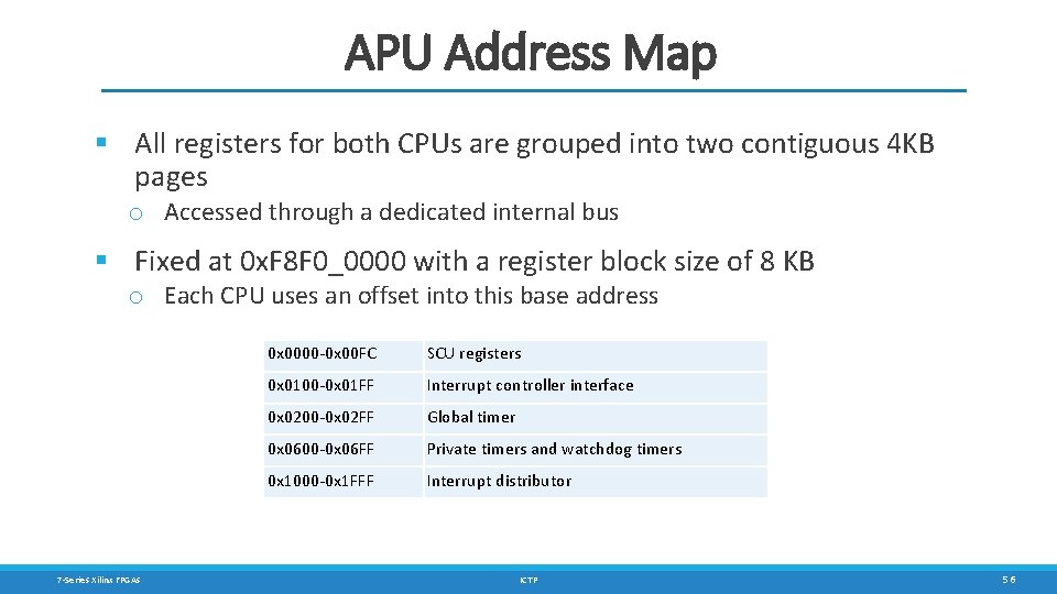
APU Address Map § All registers for both CPUs are grouped into two contiguous 4 KB pages o Accessed through a dedicated internal bus § Fixed at 0 x. F 8 F 0_0000 with a register block size of 8 KB o Each CPU uses an offset into this base address 7 -Series Xilinx FPGAs 0 x 0000 -0 x 00 FC SCU registers 0 x 0100 -0 x 01 FF Interrupt controller interface 0 x 0200 -0 x 02 FF Global timer 0 x 0600 -0 x 06 FF Private timers and watchdog timers 0 x 1000 -0 x 1 FFF Interrupt distributor ICTP 56

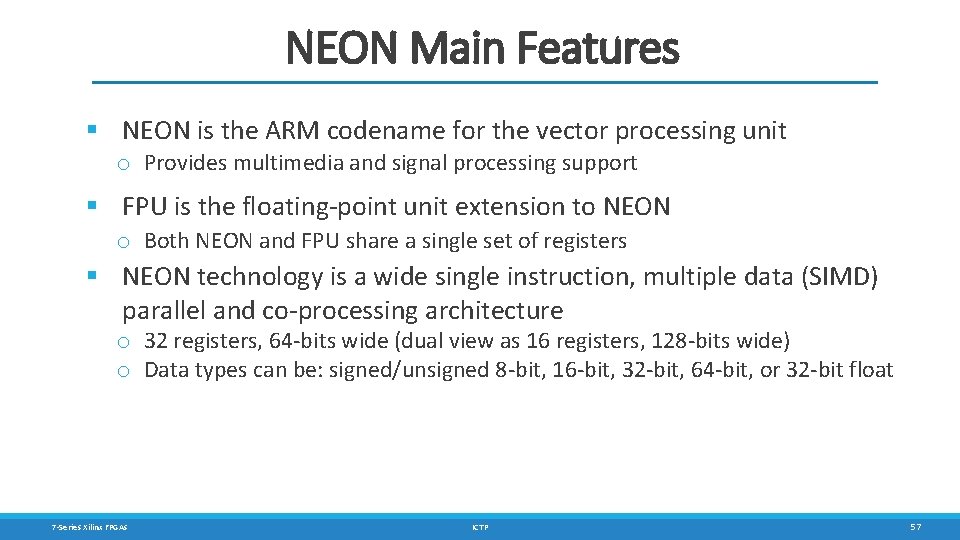
NEON Main Features § NEON is the ARM codename for the vector processing unit o Provides multimedia and signal processing support § FPU is the floating-point unit extension to NEON o Both NEON and FPU share a single set of registers § NEON technology is a wide single instruction, multiple data (SIMD) parallel and co-processing architecture o 32 registers, 64 -bits wide (dual view as 16 registers, 128 -bits wide) o Data types can be: signed/unsigned 8 -bit, 16 -bit, 32 -bit, 64 -bit, or 32 -bit float 7 -Series Xilinx FPGAs ICTP 57

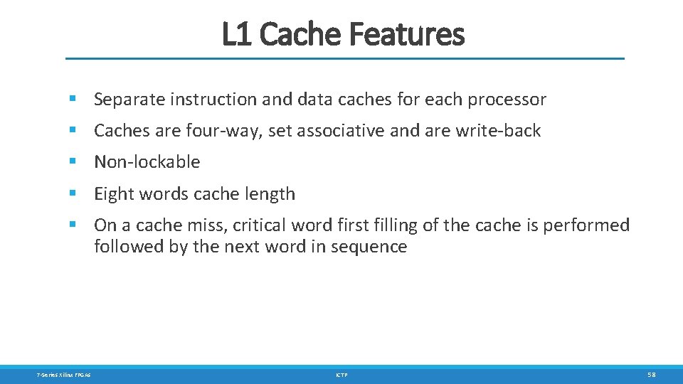
L 1 Cache Features § Separate instruction and data caches for each processor § Caches are four-way, set associative and are write-back § Non-lockable § Eight words cache length § On a cache miss, critical word first filling of the cache is performed followed by the next word in sequence 7 -Series Xilinx FPGAs ICTP 58

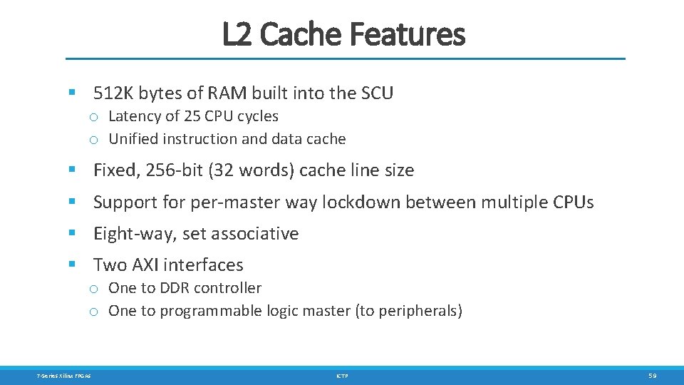
L 2 Cache Features § 512 K bytes of RAM built into the SCU o Latency of 25 CPU cycles o Unified instruction and data cache § Fixed, 256 -bit (32 words) cache line size § Support for per-master way lockdown between multiple CPUs § Eight-way, set associative § Two AXI interfaces o One to DDR controller o One to programmable logic master (to peripherals) 7 -Series Xilinx FPGAs ICTP 59

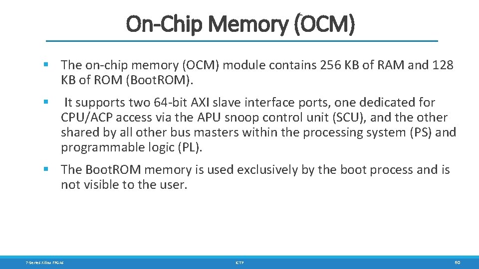
On-Chip Memory (OCM) § The on-chip memory (OCM) module contains 256 KB of RAM and 128 KB of ROM (Boot. ROM). § It supports two 64 -bit AXI slave interface ports, one dedicated for CPU/ACP access via the APU snoop control unit (SCU), and the other shared by all other bus masters within the processing system (PS) and programmable logic (PL). § The Boot. ROM memory is used exclusively by the boot process and is not visible to the user. 7 -Series Xilinx FPGAs ICTP 60

Snoop Control Unit (SCU) § Shares and arbitrates functions between the two processor cores o o o 7 -Series Xilinx FPGAs Data cache coherency between the processors Initiates L 2 AXI memory access Arbitrates between the processors requesting L 2 accesses Manages ACP accesses A second master port with programmable address filtering between OCM and L 2 memory support ICTP 61

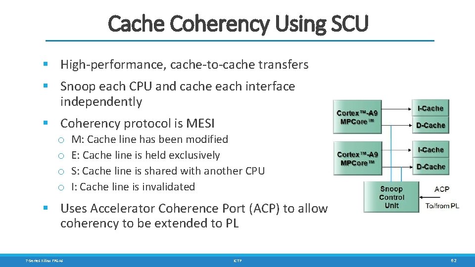
Cache Coherency Using SCU § High-performance, cache-to-cache transfers § Snoop each CPU and cache each interface independently § Coherency protocol is MESI o o M: Cache line has been modified E: Cache line is held exclusively S: Cache line is shared with another CPU I: Cache line is invalidated § Uses Accelerator Coherence Port (ACP) to allow coherency to be extended to PL 7 -Series Xilinx FPGAs ICTP 62

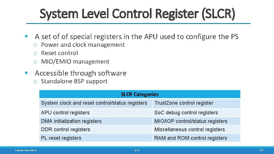
System Level Control Register (SLCR) § A set of of special registers in the APU used to configure the PS o Power and clock management o Reset control o MIO/EMIO management § Accessible through software o Standalone BSP support SLCR Categories 7 -Series Xilinx FPGAs System clock and reset control/status registers Trust. Zone control register APU control registers So. C debug control registers DMA initialization registers MIO/IOP control/status registers DDR control registers Miscellaneous control registers PL reset registers RAM and ROM control registers ICTP 63

Zynq Clocks 7 -Series Xilinx FPGAs ICTP 64

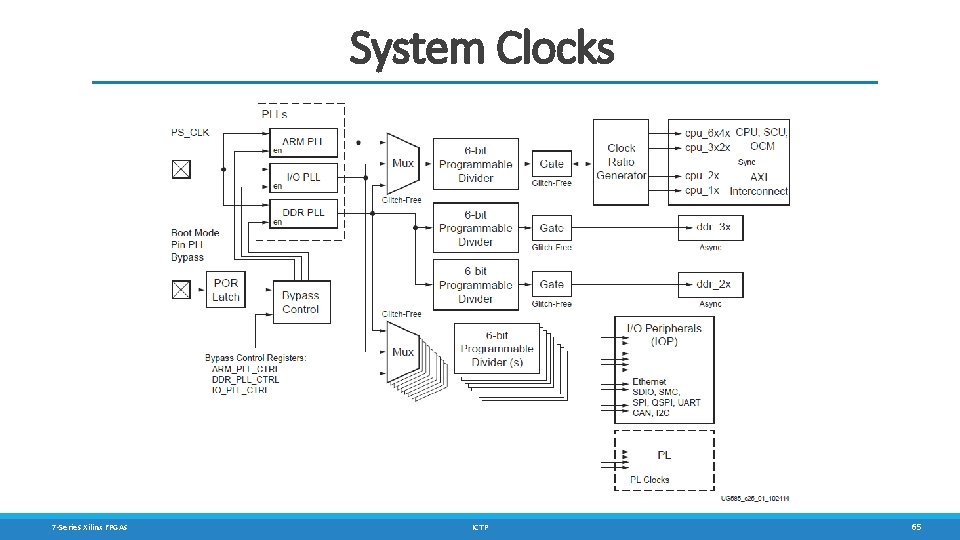
System Clocks 7 -Series Xilinx FPGAs ICTP 65

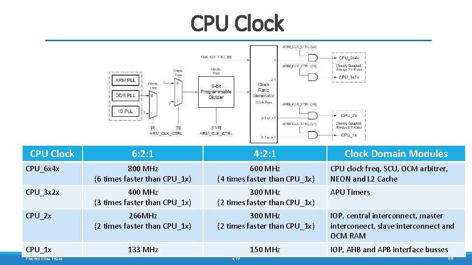
CPU Clock 6: 2: 1 4: 2: 1 CPU_6 x 4 x 800 MHz (6 times faster than CPU_1 x) 600 MHz (4 times faster than CPU_1 x) CPU clock freq, SCU, OCM arbitrer, NEON and L 2 Cache CPU_3 x 2 x 400 MHz (3 times faster than CPU_1 x) 300 MHz (2 times faster than CPU_1 x) APU Timers CPU_2 x 266 MHz (2 times faster than CPU_1 x) 300 MHz (2 times faster than CPU_1 x) IOP, central interconnect, master interconeect, slave interconnect and OCM RAM CPU_1 x 133 MHz 150 MHz 7 -Series Xilinx FPGAs ICTP Clock Domain Modules IOP, AHB and APB interface busses 66

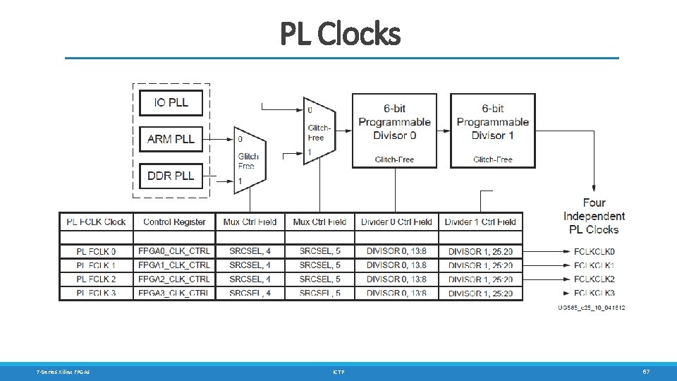
PL Clocks 7 -Series Xilinx FPGAs ICTP 67