Zerocurrent Switching Quasiresonant Converters Problems of classical DCDC
Zero-current Switching Quasiresonant Converters
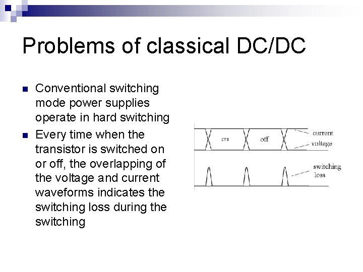
Problems of classical DC/DC n n Conventional switching mode power supplies operate in hard switching Every time when the transistor is switched on or off, the overlapping of the voltage and current waveforms indicates the switching loss during the switching
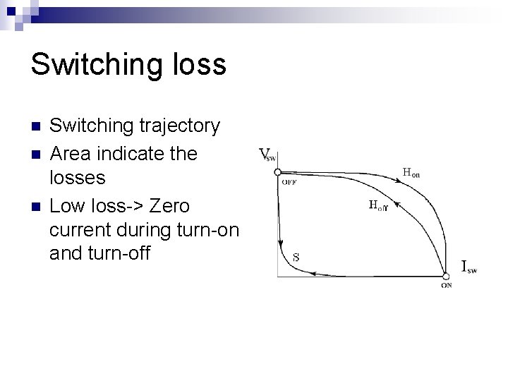
Switching loss n n n Switching trajectory Area indicate the losses Low loss-> Zero current during turn-on and turn-off
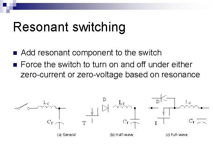
Resonant switching n n Add resonant component to the switch Force the switch to turn on and off under either zero-current or zero-voltage based on resonance (a) General (b) Half-wave (c) Full-wave
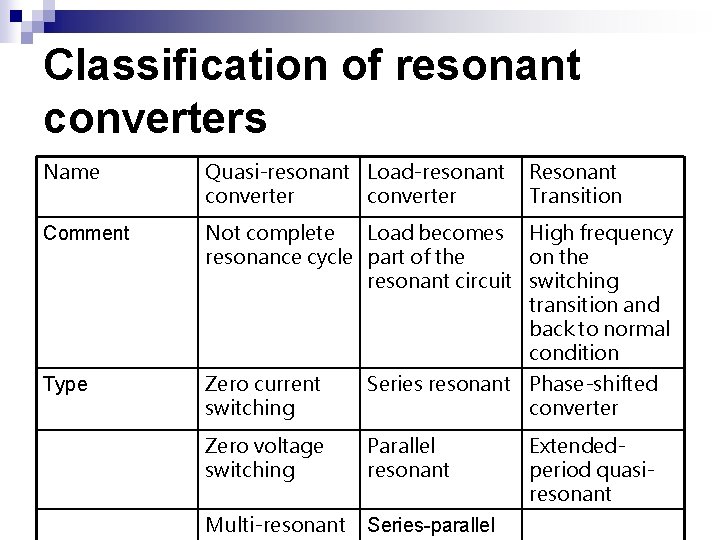
Classification of resonant converters Name Quasi-resonant Load-resonant converter Resonant Transition Comment Not complete Load becomes High frequency resonance cycle part of the on the resonant circuit switching transition and back to normal condition Type Zero current switching Series resonant Phase-shifted converter Zero voltage switching Parallel resonant Multi-resonant Series-parallel Extendedperiod quasiresonant
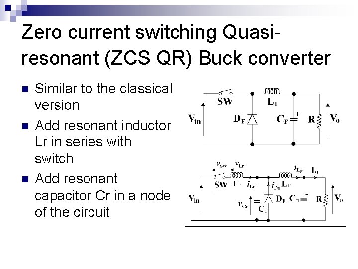
Zero current switching Quasiresonant (ZCS QR) Buck converter n n n Similar to the classical version Add resonant inductor Lr in series with switch Add resonant capacitor Cr in a node of the circuit
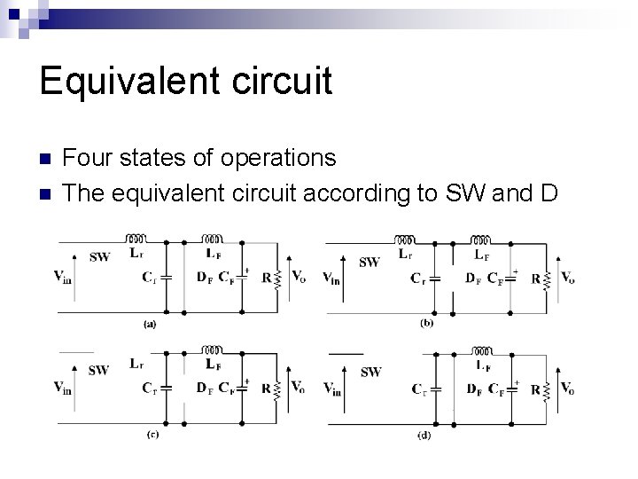
Equivalent circuit n n Four states of operations The equivalent circuit according to SW and D
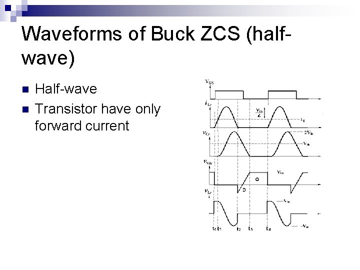
Waveforms of Buck ZCS (halfwave) n n Half-wave Transistor have only forward current
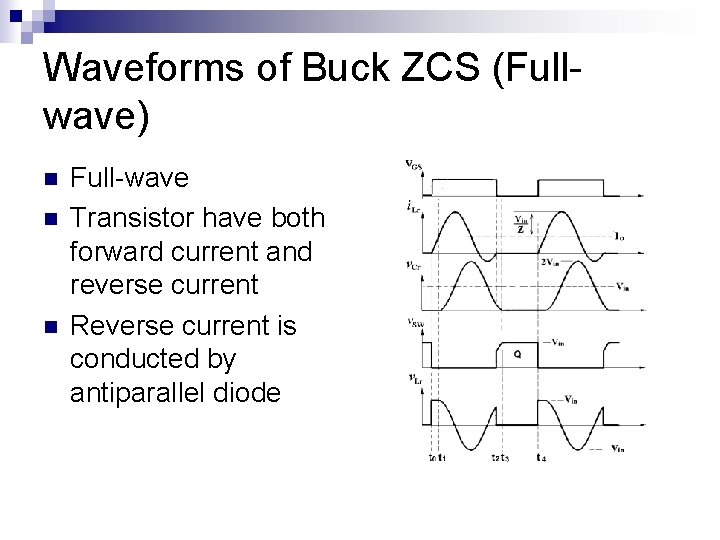
Waveforms of Buck ZCS (Fullwave) n n n Full-wave Transistor have both forward current and reverse current Reverse current is conducted by antiparallel diode
Stages of operation Linear state (Fig. 5 a) n Resonant state (Fig. 5 b) n Recovering state (Fig 5 c) n Freewheeling State (Fig 5 d) n
![Linear stage [t 0 -t 1] (Fig. 5 a) n n When Switch SW Linear stage [t 0 -t 1] (Fig. 5 a) n n When Switch SW](http://slidetodoc.com/presentation_image_h2/47903c0ec8bf7acaca2536c9c981c568/image-11.jpg)
Linear stage [t 0 -t 1] (Fig. 5 a) n n When Switch SW is turned on at t 0, freewheeling diode DF is still conducting the load current Io through LF in the previous stage The voltage across Lr is therefore equal to Vin. Input current i. Lr rises linearly and is governed by the state equations: Solution: i. Lr = Vin (t-to) /Lr
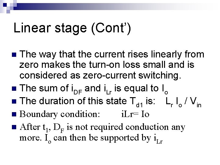
Linear stage (Cont’) The way that the current rises linearly from zero makes the turn-on loss small and is considered as zero-current switching. n The sum of i. DF and i. Lr is equal to Io n The duration of this state Td 1 is: Lr Io / Vin n Boundary condition: i. Lr= Io n After t 1, DF is not required conduction any more. Io can then be supported by i. Lr n
![Resonant state [t 1 -t 2] (Fig. 5 b) n Lr and Cr resonate Resonant state [t 1 -t 2] (Fig. 5 b) n Lr and Cr resonate](http://slidetodoc.com/presentation_image_h2/47903c0ec8bf7acaca2536c9c981c568/image-13.jpg)
Resonant state [t 1 -t 2] (Fig. 5 b) n Lr and Cr resonate and DF is off. The state equations are: n The solution is: n where
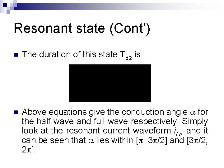
Resonant state (Cont’) n The duration of this state Td 2 is: n Above equations give the conduction angle for the half-wave and full-wave respectively. Simply look at the resonant current waveform i. Lr, and it can be seen that lies within [ , 3 /2] and [3 /2, 2 ].
Finish of the Resonant Stage n n For the half-wave mode, because there is a diode in series with the transistor, the current cannot be reversed. Therefore when the resonant current starts to enter the negative value, the diode stops conduction as shown in Fig 6 a. The resonant state then finishes For the full-wave mode, a diode is connected in parallel with the transistor. When the resonant current i. Lr changes to negative, the diode conducts. During this time, the transistor can be turned off so that when the resonant current cannot be conducted again when i. Lr returns from negative back to positive as shown in Fig. 6 b
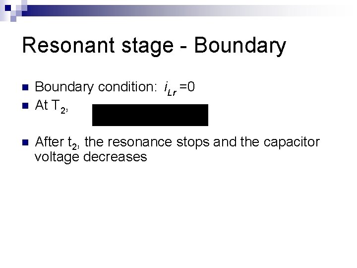
Resonant stage - Boundary n n n Boundary condition: i. Lr =0 At T 2, After t 2, the resonance stops and the capacitor voltage decreases
![Recovering stage [t 2, t 3] (Fig. 5 c n Resonant stops, Cr begins Recovering stage [t 2, t 3] (Fig. 5 c n Resonant stops, Cr begins](http://slidetodoc.com/presentation_image_h2/47903c0ec8bf7acaca2536c9c981c568/image-17.jpg)
Recovering stage [t 2, t 3] (Fig. 5 c n Resonant stops, Cr begins to be discharged through LF with a discharging current equal to Io. Solution: n n Cr is discharged until its voltage reaches zero and DF then becomes forward bias. The duration of this state can be solved by equating above equation to zero.
Boundary condition Duration: Td 3= Cr Vin (1 -cos )/Io n Boundary condition: v. Cr=0 n After t 3, Capacitor reaches zero, the stop discharging n This stage finishes n
![Free-wheeling stage [t 3, t 4] (Fig. 5 d): Output current freewheels through the Free-wheeling stage [t 3, t 4] (Fig. 5 d): Output current freewheels through the](http://slidetodoc.com/presentation_image_h2/47903c0ec8bf7acaca2536c9c981c568/image-19.jpg)
Free-wheeling stage [t 3, t 4] (Fig. 5 d): Output current freewheels through the diode DF n Duration: Td 4= Ts-Td 1 -Td 2 -Td 3 n Ts is the duration of the switching cycle. n At t 4, the converter will be turned on again and the same cycle repeats again, i. e. t 4 is the same as t 0 in the next cycle. n
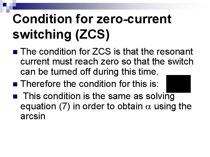
Condition for zero-current switching (ZCS) The condition for ZCS is that the resonant current must reach zero so that the switch can be turned off during this time. n Therefore the condition for this is: n This condition is the same as solving equation (7) in order to obtain using the arcsin n
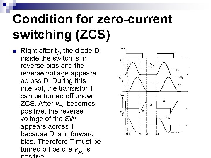
Condition for zero-current switching (ZCS) n Right after t 2, the diode D inside the switch is in reverse bias and the reverse voltage appears across D. During this interval, the transistor T can be turned off under ZCS. After vsw becomes positive, the reverse voltage of the SW appears across T because D is in forward bias. Therefore T must be turned off before vsw is
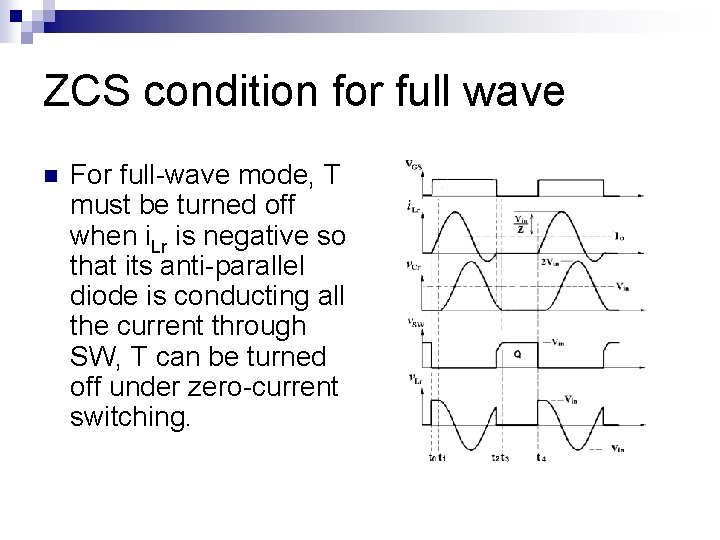
ZCS condition for full wave n For full-wave mode, T must be turned off when i. Lr is negative so that its anti-parallel diode is conducting all the current through SW, T can be turned off under zero-current switching.
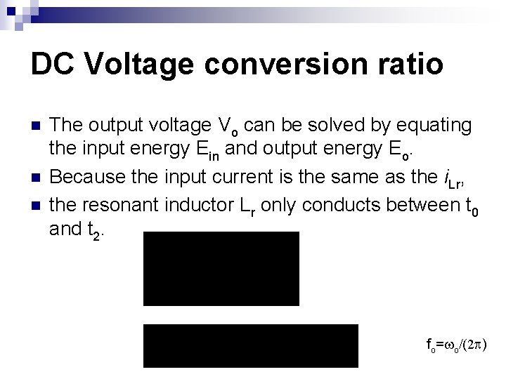
DC Voltage conversion ratio n n n The output voltage Vo can be solved by equating the input energy Ein and output energy Eo. Because the input current is the same as the i. Lr, the resonant inductor Lr only conducts between t 0 and t 2. fo= o/(2 )
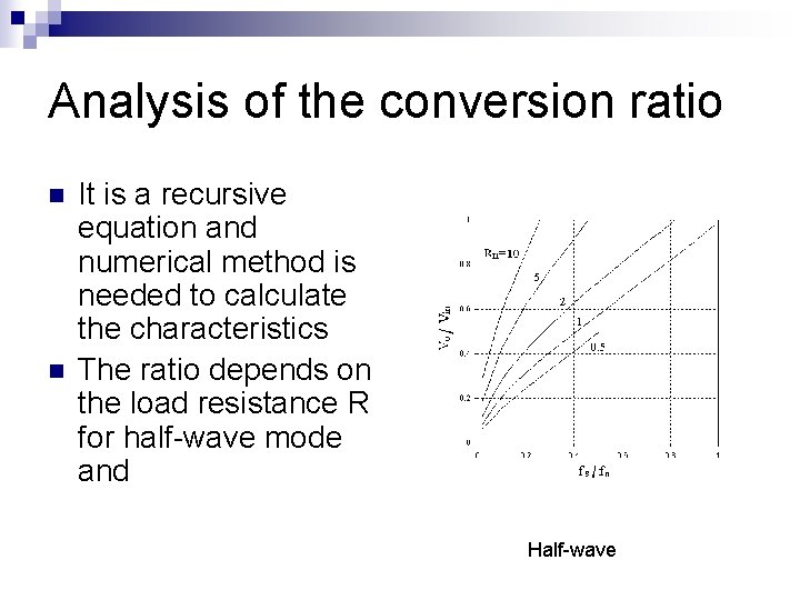
Analysis of the conversion ratio n n It is a recursive equation and numerical method is needed to calculate the characteristics The ratio depends on the load resistance R for half-wave mode and Half-wave
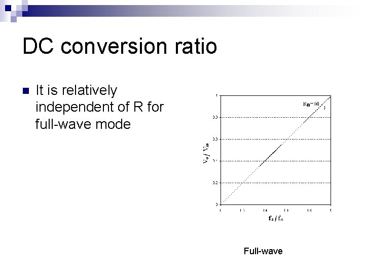
DC conversion ratio n It is relatively independent of R for full-wave mode Full-wave
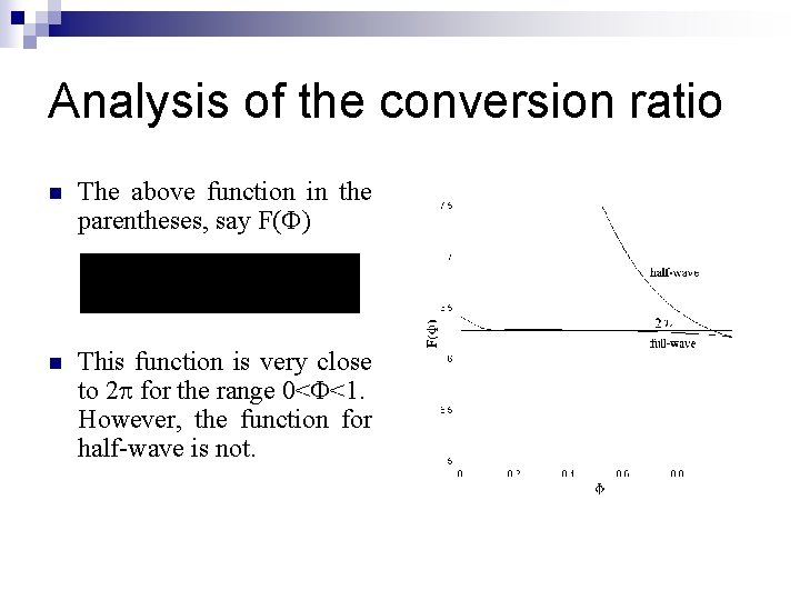
Analysis of the conversion ratio n The above function in the parentheses, say F( ) n This function is very close to 2 for the range 0< <1. However, the function for half-wave is not.
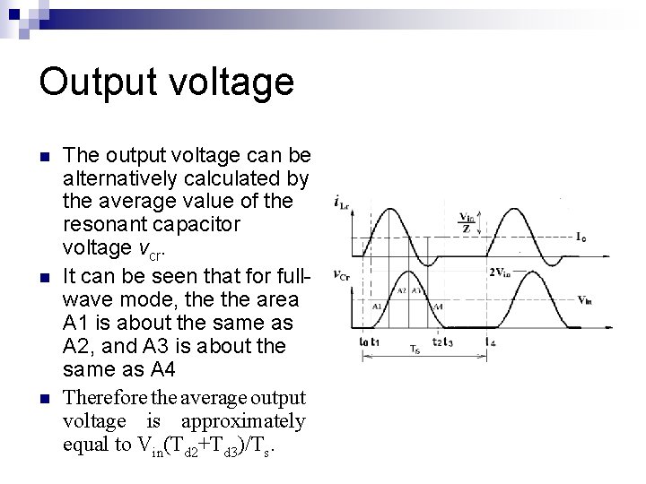
Output voltage n n n The output voltage can be alternatively calculated by the average value of the resonant capacitor voltage vcr. It can be seen that for fullwave mode, the area A 1 is about the same as A 2, and A 3 is about the same as A 4 Therefore the average output voltage is approximately equal to Vin(Td 2+Td 3)/Ts.
Conclusion + Discussion The Buck ZCS-QR converter is one of the famous resonant converters for many power conversion applications. n It also has a forward converter counterpart which is the transformer isolated version. n The converter is easy to use and usually very stable in operation. n
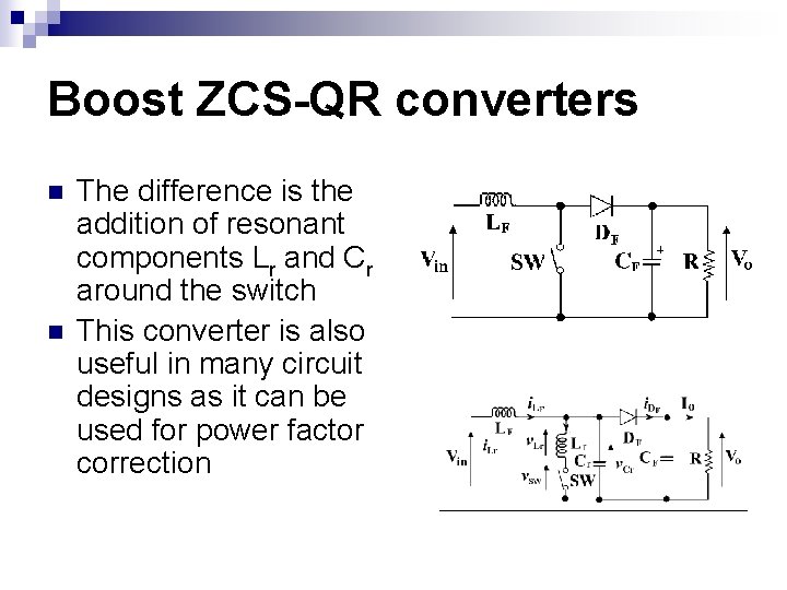
Boost ZCS-QR converters n n The difference is the addition of resonant components Lr and Cr around the switch This converter is also useful in many circuit designs as it can be used for power factor correction
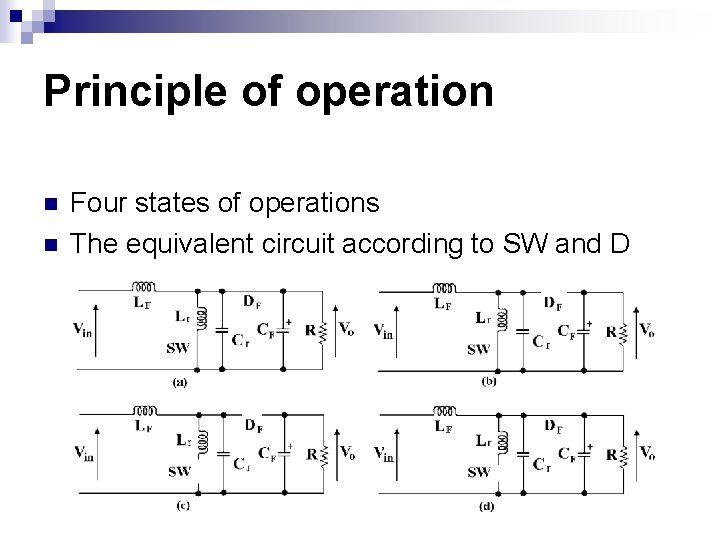
Principle of operation n n Four states of operations The equivalent circuit according to SW and D
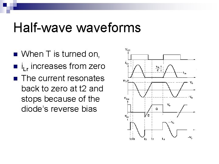
Half-waveforms n n n When T is turned on, i. Lr increases from zero The current resonates back to zero at t 2 and stops because of the diode’s reverse bias
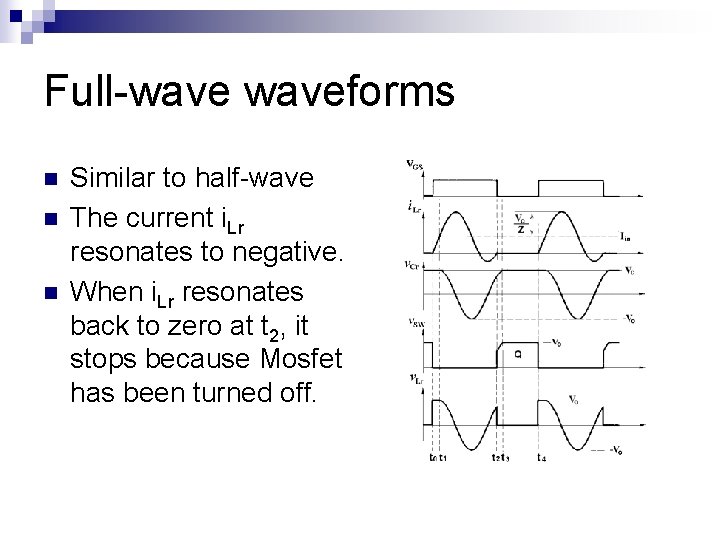
Full-waveforms n n n Similar to half-wave The current i. Lr resonates to negative. When i. Lr resonates back to zero at t 2, it stops because Mosfet has been turned off.
![Linear stage [t 0 -t 1] (Fig. 11 a): n n When switch SW Linear stage [t 0 -t 1] (Fig. 11 a): n n When switch SW](http://slidetodoc.com/presentation_image_h2/47903c0ec8bf7acaca2536c9c981c568/image-33.jpg)
Linear stage [t 0 -t 1] (Fig. 11 a): n n When switch SW is turned on at t 0, freewheeling diode DF is still conducting the source current Iin through LF. The current i. DF is also equal to Iin at t 0. The voltage across v. Cr is therefore equal to Vo. i. Lr = Vo (t-t 0) /Lr n n When t>t 0, i. DF decreases such that it is equal to Iin-i. Lr.
Linear stage (Boundary) This state finishes when i. Lr increases until i. Lr is greater than Iin. i. DF decreases to zero. n DF is not required for conduction any more. Iin can then be supported by i. Lr which is shown in next state. n The duration of this state Td 1 is: Lr Iin / Vo n Boundary condition: i. Lr=Iin n
![Resonant state [t 1 -t 2] (Fig. 11 b): n Lr and Cr resonate Resonant state [t 1 -t 2] (Fig. 11 b): n Lr and Cr resonate](http://slidetodoc.com/presentation_image_h2/47903c0ec8bf7acaca2536c9c981c568/image-35.jpg)
Resonant state [t 1 -t 2] (Fig. 11 b): n Lr and Cr resonate and DF is off. The state equations are: n Solution:
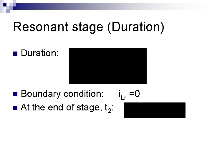
Resonant stage (Duration) n Duration: Boundary condition: i. Lr =0 n At the end of stage, t 2: n
![Recovering stage [t 2, t 3] (Fig. 10 c): n Resonant stops, Cr begins Recovering stage [t 2, t 3] (Fig. 10 c): n Resonant stops, Cr begins](http://slidetodoc.com/presentation_image_h2/47903c0ec8bf7acaca2536c9c981c568/image-37.jpg)
Recovering stage [t 2, t 3] (Fig. 10 c): n Resonant stops, Cr begins to be charged by the input current Iin through LF. n Solution:
Recovering stage (how to end) Cr is discharged until its voltage reaches zero and DF then becomes forward bias n The duration of this state can be solved by equating equation (42) to zero. n Duration: Td 3= Cr Vo (1 -cos )/Iin n Boundary condition: v. Cr=Vo n
![Freewheeling stage [t 3, t 4] (Fig. 10 d): Output current freewheels through DF. Freewheeling stage [t 3, t 4] (Fig. 10 d): Output current freewheels through DF.](http://slidetodoc.com/presentation_image_h2/47903c0ec8bf7acaca2536c9c981c568/image-39.jpg)
Freewheeling stage [t 3, t 4] (Fig. 10 d): Output current freewheels through DF. n This stage finishes when the control gate voltage of SW is turned on again at t 4. n Duration: Td 4= Ts-Td 1 -Td 2 -Td 3 n
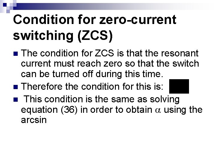
Condition for zero-current switching (ZCS) The condition for ZCS is that the resonant current must reach zero so that the switch can be turned off during this time. n Therefore the condition for this is: n This condition is the same as solving equation (36) in order to obtain using the arcsin n
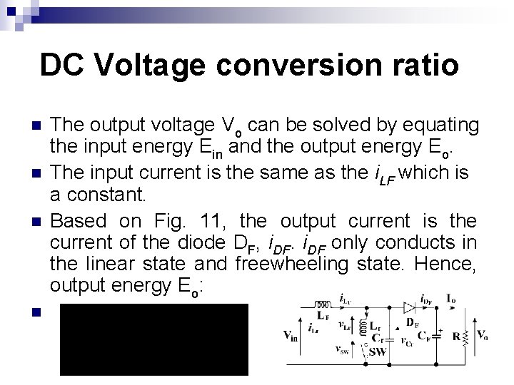
DC Voltage conversion ratio n n The output voltage Vo can be solved by equating the input energy Ein and the output energy Eo. The input current is the same as the i. LF which is a constant. Based on Fig. 11, the output current is the current of the diode DF, i. DF only conducts in the linear state and freewheeling state. Hence, output energy Eo:
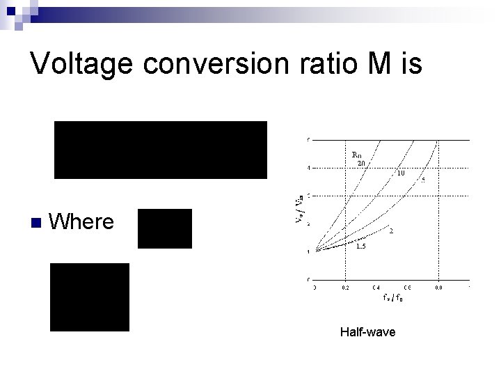
Voltage conversion ratio M is n Where Half-wave
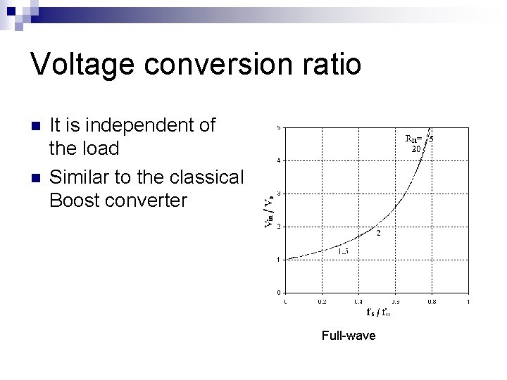
Voltage conversion ratio n n It is independent of the load Similar to the classical Boost converter Full-wave
Comment + Discussion The function in the parentheses, is the same format as F( ) n The transistor’s source pin shares a common ground n Similar to the other advantage and disadvantage of classical Boost convetrer n
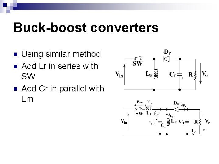
Buck-boost converters n n n Using similar method Add Lr in series with SW Add Cr in parallel with Lm
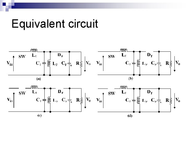
Equivalent circuit
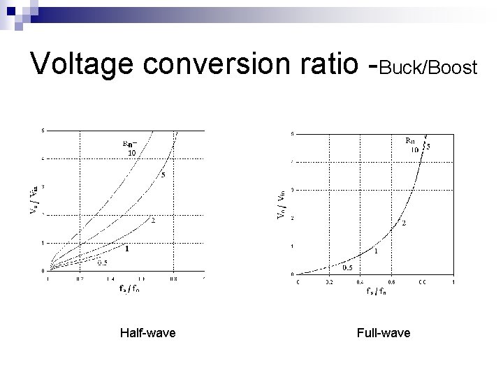
Voltage conversion ratio -Buck/Boost Half-wave Full-wave
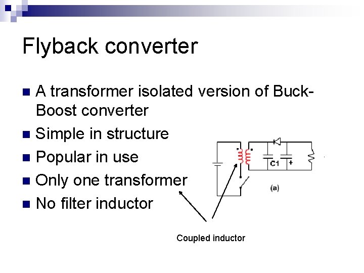
Flyback converter A transformer isolated version of Buck. Boost converter n Simple in structure n Popular in use n Only one transformer n No filter inductor n Coupled inductor
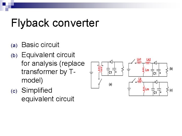
Flyback converter (a) (b) (c) Basic circuit Equivalent circuit for analysis (replace transformer by Tmodel) Simplified equivalent circuit
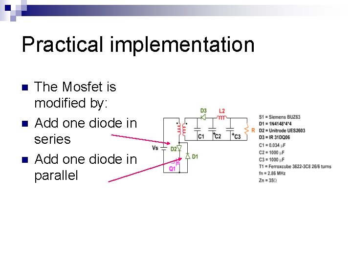
Practical implementation n The Mosfet is modified by: Add one diode in series Add one diode in parallel
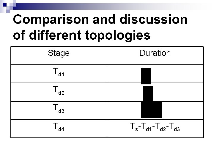
Comparison and discussion of different topologies Stage Duration Td 1 Td 2 Td 3 Td 4 Ts-Td 1 -Td 2 -Td 3
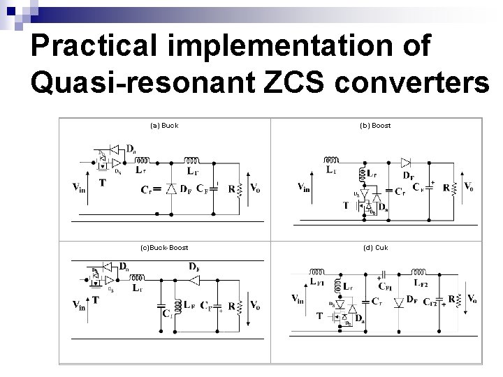
Practical implementation of Quasi-resonant ZCS converters (a) Buck (b) Boost (c)Buck-Boost (d) Cuk
Tutorial n n n A full-wave zero-current switching quasi-resonant buck converter is operated at the following specification: Input voltage VS=50 V, Output voltage Vo=20 V Switching frequency fs=500 k. Hz, Output current Io = 10 A n n Calculate the requirement of the resonant component Lr and Cr. Estimate the power loss in the Lr if its series equivalent resistance is 0. 1. (answ: Lr=0. 637 H, Cr=0. 127 F, loss=6 W)
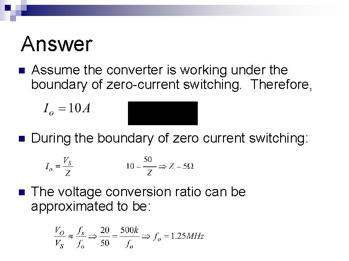
Answer n Assume the converter is working under the boundary of zero-current switching. Therefore, n During the boundary of zero current switching: n The voltage conversion ratio can be approximated to be:
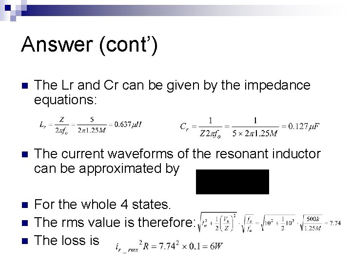
Answer (cont’) n The Lr and Cr can be given by the impedance equations: n The current waveforms of the resonant inductor can be approximated by n For the whole 4 states. The rms value is therefore: The loss is n n
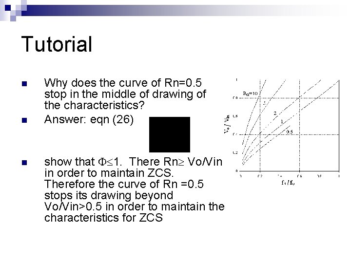
Tutorial n n n Why does the curve of Rn=0. 5 stop in the middle of drawing of the characteristics? Answer: eqn (26) show that 1. There Rn Vo/Vin in order to maintain ZCS. Therefore the curve of Rn =0. 5 stops its drawing beyond Vo/Vin>0. 5 in order to maintain the characteristics for ZCS
- Slides: 56